University of Houston Engineers Develop a Thin Film That Makes AI Chips Faster and Far More Energy Efficient

Artificial intelligence is advancing at a staggering pace, but behind every breakthrough model and lightning-fast response time is an enormous energy bill. Modern AI systems demand vast computing power, and that power comes with a serious downside: heat, inefficiency, and soaring electricity consumption. Engineers at the University of Houston (UH) believe they have found a promising solution, and it comes in the form of an ultra-thin material designed to fundamentally change how AI chips handle electricity.
Researchers at UH have developed a two-dimensional thin-film dielectric material that could make AI hardware run faster, cooler, and far more efficiently. The work directly targets one of the biggest bottlenecks in AI computing today—energy loss inside integrated circuit chips—and proposes a material-level fix rather than a software workaround.
Why AI Chips Consume So Much Power
AI workloads rely on high-speed, high-frequency electrical signals moving through densely packed circuits. These circuits are made of conductors separated by insulating materials known as dielectrics. Traditional dielectrics tend to store electrical energy during operation, and much of that stored energy is later released as waste heat.
This heat is not just a minor inconvenience. AI data centers now rely on massive cooling systems that consume large amounts of electricity just to keep chips within safe operating temperatures. Excess heat also slows down signal transmission, increases response times, and shortens chip lifespan. As AI adoption grows, this problem scales rapidly.
The Core Idea Behind the New Thin Film
The UH team focused on developing a low-k dielectric, where “k” refers to dielectric permittivity—a measure of how much electrical energy a material stores. Lower k values mean less stored energy, less heat, and faster signal propagation.
Instead of using conventional insulating materials, the researchers turned to covalent organic frameworks (COFs). These are lightweight, carbon-based materials made from light elements such as carbon, hydrogen, nitrogen, and oxygen, arranged in highly ordered, porous crystalline structures.
The resulting thin film is two-dimensional, meaning it forms sheet-like layers that are only nanometers thick. Crucially, the material does not store electricity, which dramatically reduces heat generation during high-speed operation.
Who Led the Research
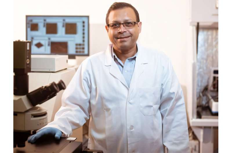
The project was led by Alamgir Karim, Dow Chair and Welch Foundation Professor in the William A. Brookshire Department of Chemical and Biomolecular Engineering at the University of Houston. A major contributor to the work was Maninderjeet Singh, who developed the material during his doctoral research at UH and is now a postdoctoral researcher at Columbia University.
Other collaborators included Devin Shaffer, a UH professor of civil engineering, doctoral student Erin Schroeder, and student researcher Saurabh Tiwary, who focused on studying the electronic properties of the films for next-generation chip applications.
How the Material Was Made
The thin films were created using a technique known as synthetic interfacial polymerization. In this process, molecular building blocks are dissolved into two liquids that do not mix. At the interface between these liquids, the molecules react and “stitch” themselves together into strong, crystalline, sheet-like structures.
This approach allows researchers to precisely control thickness, structure, and uniformity—key requirements for materials that need to integrate seamlessly into advanced semiconductor manufacturing.
The method itself builds on foundational work in organic framework chemistry pioneered by Omar M. Yaghi, whose research into COFs and related materials earned global recognition, including a 2025 Nobel Prize in Chemistry for contributions to framework-based materials science.
What Makes This Thin Film Special
The UH team didn’t just create a novel material—they rigorously tested it for real-world electronic performance. Their findings showed a combination of properties rarely achieved together in a single dielectric material.
The new 2D COF films demonstrated:
- An ultralow dielectric constant, meaning minimal energy storage
- Ultrahigh electrical breakdown strength, allowing them to operate safely under high voltages
- Excellent thermal stability, even at elevated operating temperatures
- Strong mechanical and structural integrity, critical for long-term device reliability
These characteristics make the material especially suitable for high-power and high-frequency AI devices, where conventional dielectrics struggle.
Why Low-k Materials Matter for AI
In modern chips, dielectrics sit between metal interconnects that carry electrical signals. If the dielectric stores too much energy, it causes signal delay, interference (cross-talk), and heat buildup.
By using low-k materials, engineers can:
- Speed up signal transmission
- Reduce power consumption
- Minimize interference between adjacent circuits
- Allow chips to run cooler and faster
For AI processors, which push hardware to its limits, these improvements can translate into significant performance gains and lower operating costs.
Implications for AI Data Centers
One of the biggest beneficiaries of this research could be AI data centers, which already account for a growing share of global electricity usage. Cooling alone can represent a major fraction of a data center’s power consumption.
By reducing heat generation at the chip level, this thin-film technology could:
- Lower the need for energy-intensive cooling infrastructure
- Improve chip longevity and reliability
- Reduce overall energy consumption per AI task
As AI continues to expand into cloud services, autonomous systems, and large-scale machine learning, such material-level efficiency gains become increasingly important.
Beyond AI Chips: Broader Applications
While AI is a major focus, the implications of this work extend to conventional electronics as well. Any device that relies on high-speed integrated circuits—such as telecommunications hardware, power electronics, and advanced computing systems—could benefit from low-k, high-strength dielectric materials.
The combination of porosity, lightweight composition, and stability also opens the door to future innovations in flexible electronics and next-generation semiconductor architectures.
A Step Toward More Sustainable Computing
The rapid growth of AI has sparked concerns about its environmental footprint. Material innovations like this one represent a hardware-level approach to sustainability, addressing energy efficiency at its source rather than compensating for inefficiency later with larger cooling systems.
By rethinking the fundamental materials used inside chips, the University of Houston team has demonstrated a pathway toward faster AI with a smaller energy cost—a balance the industry urgently needs.
Research Reference
Two-Dimensional Covalent Organic Framework Films for High Dielectric Strength Electrically and Thermo-Mechanically Stable Low Permittivity Dielectrics, ACS Nano (2025)
https://doi.org/10.1021/acsnano.5c11582


