Electrons Mostly Stay in Their Own Layers in Mismatched Quantum Materials, Scientists Find

Researchers at Cornell University have uncovered a crucial insight into how electrons behave inside a special class of quantum materials known as misfit layered compounds. These materials are made by stacking layers whose atomic grids do not line up neatly—imagine snapping together LEGO pieces with different shapes. For years, scientists believed that this mismatch caused electrons to jump from one layer to another. The new research shows something very different: most electrons actually stay in their original layers, even though their energy levels change significantly.
This finding reshapes how physicists understand charge transfer in complex materials and could directly influence the future design of superconductors, electronic cooling devices, and other advanced quantum technologies.
What Are Misfit Quantum Materials?
Misfit materials belong to a broader family called incommensurate layered materials. In simple terms, these are solids made from alternating atomic layers that have different crystal symmetries and lattice spacings. One layer might form a square grid, while the neighboring layer forms a hexagonal one. Because their atomic patterns do not align perfectly, the layers are said to be “incommensurate.”
In the study, researchers focused on misfit layered heterostructures that alternate between:
- A rare-earth metal rock-salt layer with square symmetry
- A transition metal dichalcogenide layer with hexagonal symmetry
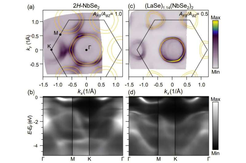
A key example examined was the compound (LaSe)1.14(NbSe2)2, compared against undoped 2H-NbSe2, a well-known layered material.
These systems are not just structural curiosities. Incommensurate materials are known to host exotic electronic behaviors, making them valuable platforms for exploring superconductivity and other quantum effects.
The Long-Standing Assumption About Electron Transfer
For decades, experimental measurements—especially using Angle-Resolved Photoemission Spectroscopy (ARPES)—showed large shifts in energy bands when different layers were stacked together in misfit compounds. These shifts were widely interpreted as evidence that electrons were physically moving from one layer to another, creating significant charge transfer between layers.
This assumption became deeply embedded in the literature. If energy bands moved, the thinking went, electrons must be relocating in large numbers. But that interpretation was never directly proven—until now.
A New Computational Method Changes the Picture
The Cornell team introduced a new computational approach called MINT-Sandwich, developed by doctoral researcher Drake Niedzielski under the guidance of physicist Tomás Arias.
This method is built on a powerful but often overlooked idea: electrons mostly respond to their immediate local environment, rather than the entire material at once. By focusing on local interactions, MINT-Sandwich can accurately calculate both the energy and real-space location of electrons in incommensurate systems.
Crucially, the method avoids introducing artificial strain, a common workaround in earlier simulations that forced mismatched layers to fit together unnaturally. This allowed the researchers to model the materials as they actually exist.
Using this approach, the team performed what can best be described as a true experiment inside a computer, solving the underlying laws of physics rather than relying on approximations alone.
What the Calculations Revealed
When Niedzielski applied the method to a single square layer stacked against a hexagonal one, the results were surprising.
Yes, the calculations confirmed that the number of high-energy electrons in the hexagonal layer increased—just as experiments had shown. But when the researchers tracked the actual movement of electrons between layers, they found that real charge transfer was about six times smaller than previously assumed.
In other words, very few electrons actually crossed from one layer to another. Instead, electrons within each layer rearranged themselves in response to chemical bonding at the interface. This rearrangement changed energy levels and band structures without requiring large-scale electron migration.
The dramatic shifts seen in ARPES data were therefore not proof of mass electron transfer, but evidence of intralayer electronic reorganization.
Why Electrons Prefer to Stay Put
At the microscopic level, electrons behave like waves spread across a material. However, in dense systems filled with many electrons, those waves interfere and cancel out over long distances. What remains dominant is the local environment around each electron.
In misfit compounds, the chemical bonding between mismatched layers modifies this local environment. Electrons respond by adjusting their energy states within their home layer rather than jumping across the interface. This explains why the system can show strong electronic effects without significant charge movement between layers.
Experimental Support From Microscopy and ARPES
The computational findings were closely tied to experimental work. Researchers at PARADIM, a National Science Foundation–supported facility, conducted ARPES measurements to map Fermi surfaces and valence band structures in both reference and misfit materials.
Additionally, advanced microscopy led by Lena Kourkoutis and collaborators provided high-resolution images of the atomic structure. These images were essential for locating atoms precisely, allowing the calculations to be performed efficiently and accurately.
The agreement between experiment and computation strengthened confidence that the new interpretation correctly explains what is happening inside these materials.
Why This Matters for Material Design
Understanding whether electrons move between layers or simply rearrange within them is not a minor detail—it fundamentally affects how scientists design and predict material behavior.
Misfit layered materials are actively studied for their potential in:
- Superconductivity
- Thermoelectric devices
- Electronic cooling technologies
- Novel quantum electronic systems
If designers assume large charge transfer when none actually occurs, predictions about conductivity, magnetism, and superconducting behavior can be misleading. This research provides a clearer foundation for engineering materials with precisely tuned quantum properties.
How This Fits Into the Bigger Quantum Materials Picture
The work also connects to broader interest in incommensurate systems, such as magic-angle twisted bilayer graphene, where a small mismatch between layers leads to superconductivity. While misfit compounds differ structurally, they share the theme that layer mismatch can unlock new physics.
The new study shows that understanding these effects requires looking beyond simple charge-transfer models and focusing on local electronic structure and bonding.
A New Tool for Exploring the Quantum World
Beyond the specific results, MINT-Sandwich represents a major advance in computational physics. It opens the door to studying many layered materials that were previously too complex to model accurately.
As Arias emphasized, this approach stands alongside theory and experiment as a third pillar of scientific discovery, capable of answering questions that neither experiments nor traditional simulations can resolve on their own.


