Imec Integrates Colloidal Quantum Dot Photodiodes on Metasurfaces to Enable Compact and Scalable SWIR Sensors

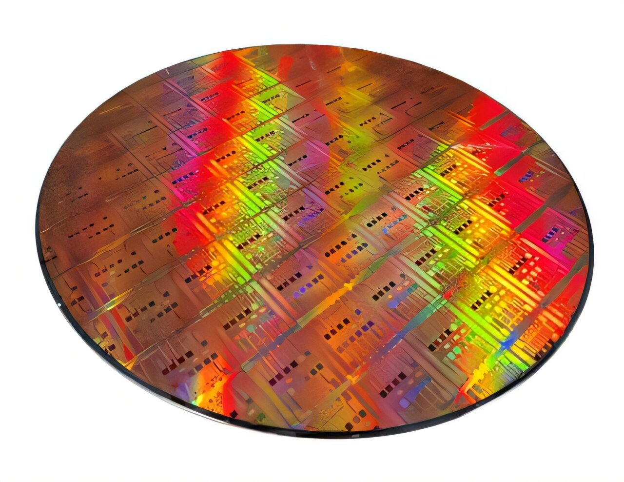
At the IEEE International Electron Devices Meeting (IEDM 2025), imec—one of the world’s leading research and innovation hubs in advanced semiconductor technologies—presented a major development in shortwave infrared (SWIR) sensing. The organization successfully demonstrated the integration of colloidal quantum dot photodiodes (QDPDs) on metasurfaces, all fabricated on 300 mm CMOS wafers. This achievement lays the foundation for a new generation of compact, high-resolution, and cost-effective SWIR spectral sensors that can be manufactured using standard semiconductor processes.
This integration represents more than a technical milestone. It addresses long-standing challenges in SWIR imaging related to size, cost, and scalability, while opening the door to customizable spectral sensors that can be adapted across a wide range of industries.
Why SWIR Sensors Matter
SWIR sensors operate beyond the visible spectrum, typically in the wavelength range of about 900 nm to 2,500 nm. In this region, light interacts with materials in ways that visible light cannot. As a result, SWIR imaging can reveal contrasts and details that remain invisible to the human eye.
For example, SWIR sensors can see through plastics, fabrics, and certain coatings, and they perform well in challenging conditions such as haze, smoke, or low-light environments. These properties make SWIR technology extremely valuable in fields like security, industrial inspection, agriculture, automotive sensing, and aerospace.
Despite these advantages, conventional SWIR sensors are often expensive, bulky, and complex to manufacture. Many rely on materials such as indium gallium arsenide (InGaAs), which are costly and difficult to integrate with mainstream CMOS manufacturing. This has limited SWIR adoption to specialized or high-budget applications.
Quantum Dot Image Sensors as an Alternative
Colloidal quantum dots (QDs) have emerged as a promising alternative for SWIR detection. These nanoscale semiconductor particles can be chemically engineered so that their absorption properties match specific infrared wavelengths. Because they can be processed from solution and deposited at relatively low temperatures, quantum dots are attractive for CMOS-compatible manufacturing.
Quantum dot image sensors already offer the potential for lower cost and higher resolution compared to traditional SWIR technologies. However, until now, most quantum dot SWIR sensors have operated in a broadband mode, meaning they detect a wide range of wavelengths rather than distinguishing between specific spectral bands. This limits their usefulness in applications that require spectral information rather than simple intensity measurements.
The Role of Metasurfaces in Spectral Control
This is where metasurfaces come into play. Metasurfaces are ultra-thin, nano-patterned structures designed to precisely control how light behaves when it interacts with a surface. By carefully engineering these patterns, metasurfaces can selectively filter, redirect, or enhance specific wavelengths of light.
Imec’s approach combines quantum dot photodiodes with CMOS-fabricated metasurfaces, allowing spectral selectivity to be defined at the CMOS and optical design level, rather than by redesigning the photodiode stack itself. This is a critical shift in how spectral sensors are built.
Traditionally, achieving different spectral responses in quantum dot image sensors requires re-engineering the photodiode layers for each wavelength, which adds complexity, cost, and development time. Imec’s solution avoids this problem by using metasurfaces to tune the spectral response instead. The underlying photodiode structure remains the same, while the metasurface determines which wavelengths are detected.
Integration on 300 mm CMOS Wafers
A key highlight of imec’s work is that the entire integration process was demonstrated on 300 mm CMOS wafers, using the organization’s advanced CMOS pilot line. This is significant because it proves the technology is compatible with industrial-scale semiconductor manufacturing.
The team demonstrated colloidal quantum dot photodiodes integrated directly on top of metasurfaces, with measured external quantum efficiency (EQE) spectra confirming that the spectral response can be effectively controlled. Scanning electron microscope (SEM) cross-sections showed the structural integrity of the integrated devices, validating both the optical and electrical performance of the architecture.
By keeping the process CMOS-compatible, imec has shown that this technology can move beyond laboratory-scale demonstrations and into real-world manufacturing environments.
Scalability and Customization as Key Advantages
One of the most important aspects of this development is scalability. Because the spectral tuning is handled by metasurfaces rather than photodiode redesign, sensor manufacturers can adapt the technology to different applications without overhauling the entire device structure.
This approach enables easily customizable, high-resolution spectral SWIR sensors that can be tailored to specific use cases. It also reduces development costs and shortens time-to-market, which are critical factors for widespread adoption.
In practical terms, this means sensor designers can create compact SWIR systems with multiple spectral channels, all integrated on a single chip, while still relying on mature CMOS fabrication infrastructure.
Potential Applications Across Industries
The implications of this technology extend across numerous sectors. In security and defense, compact spectral SWIR sensors could improve surveillance, target identification, and imaging through obscurants. In agriculture, spectral SWIR imaging can help monitor crop health, water content, and soil conditions with greater precision.
In the automotive and aerospace industries, SWIR sensors can enhance vision systems for autonomous vehicles and aircraft, particularly in low-visibility environments. Industrial inspection and material sorting could also benefit from spectral SWIR detection, enabling better identification of defects or material compositions.
Because the sensors are smaller and potentially more affordable, entirely new applications may emerge as the technology matures.
From Proof of Concept to Manufacturing
While the results presented at IEDM 2025 represent a strong proof of concept, imec is already focused on the next phase. The goal is to scale this technology from laboratory demonstrations to low-volume production, and eventually to full-scale manufacturing.
To accelerate this transition, imec is actively inviting industry partners to collaborate. By combining imec’s expertise in quantum dot image sensors, metasurfaces, spectral imaging, and advanced CMOS processing with application-specific knowledge from partners, the organization aims to bring this technology into real-world products more quickly.
The long-term vision is to establish an industry-ready platform for next-generation SWIR sensing that can be adapted, customized, and produced at scale.
A Step Forward for Spectral Imaging
The integration of colloidal quantum dot photodiodes on metasurfaces represents a meaningful step forward in spectral imaging technology. By shifting complexity away from the photodiode layer and into CMOS-compatible metasurfaces, imec has demonstrated a practical and scalable path toward compact spectral SWIR sensors.
As this platform evolves through collaboration and further development, it has the potential to reshape how SWIR imaging systems are designed, manufactured, and deployed—making advanced spectral sensing more accessible across industries.
Research paper:
https://iedm25.mapyourshow.com/8_0/sessions/session-details.cfm?ScheduleID=380


