An Earthquake on a Chip Could Make Smartphones Smaller and Faster

Engineers have figured out how to create something that sounds impossible at first: tiny, controlled earthquakes on a microchip. While these “earthquakes” won’t be shaking buildings anytime soon, they could have a serious impact on the future of smartphones, wireless devices, and radio technology.
The breakthrough comes from a team of engineers led by Matt Eichenfield, an incoming faculty member at the University of Colorado Boulder, working alongside researchers from the University of Arizona and Sandia National Laboratories. Their work introduces a new type of device known as a surface acoustic wave phonon laser, and it represents a major step forward in how chips can generate and control vibrations at extremely high frequencies.
At its core, this research is about improving how electronic devices process signals — and doing it with smaller, faster, and more efficient hardware.
What Are Surface Acoustic Waves and Why Do They Matter?
To understand why this matters, it helps to know what surface acoustic waves (SAWs) are. These waves are mechanical vibrations that travel only along the surface of a material, rather than through its entire body. In nature, earthquakes generate massive surface acoustic waves that ripple across the Earth’s surface and cause damage.
On a much smaller scale, SAWs are already deeply embedded in modern technology.
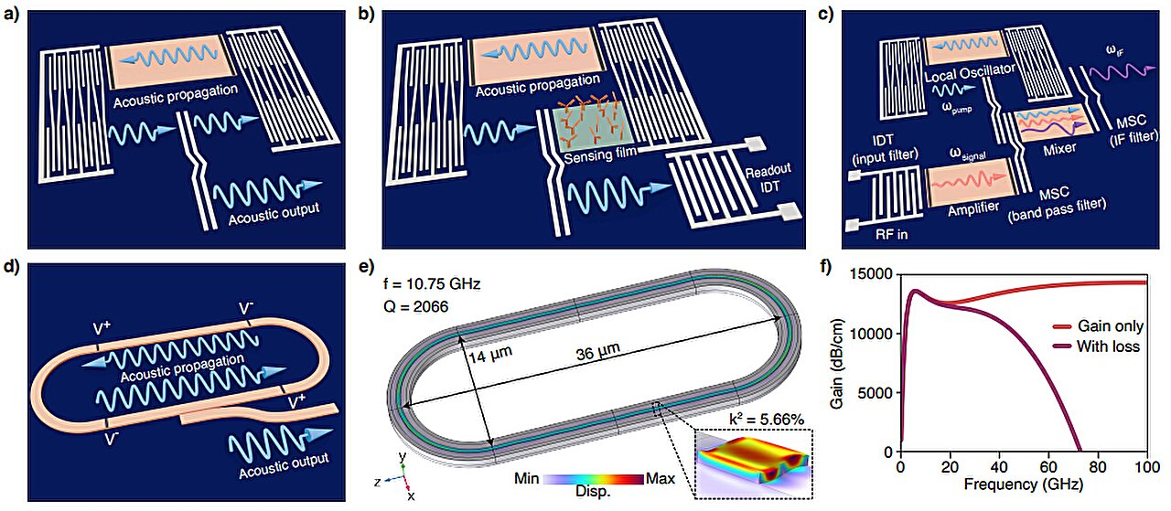
They play a critical role in cell phones, GPS receivers, garage door openers, key fobs, radar systems, and wireless communication devices. Inside a smartphone, SAWs act as filters. When a phone receives radio signals from a cell tower, those signals are converted into tiny mechanical vibrations. The chip then removes unwanted frequencies and noise before converting the vibrations back into clean radio waves.
This process happens constantly whenever you make a call, send a text, or browse the internet.
The Problem With Today’s SAW Technology
Despite how important SAWs are, current SAW devices come with limitations. Most of today’s systems require multiple chips and external power sources to generate and control these waves. They also struggle to operate efficiently at very high frequencies.
Traditional SAW devices typically top out at around 4 gigahertz, which restricts how compact and powerful wireless systems can become. As smartphones and other devices continue to shrink while demanding more performance, engineers are running into physical limits with existing designs.
This is where the new phonon laser comes in.
A Phonon Laser Instead of a Light Laser
The research team took inspiration from diode lasers, which are widely used in optical technologies. A typical diode laser works by bouncing light between two microscopic mirrors inside a semiconductor. As electricity flows through the material, atoms emit more light, amplifying the beam until a powerful, coherent laser emerges.
The engineers asked a simple but bold question: What if the same idea could work for sound-like vibrations instead of light?
The result is a phonon laser, a device that generates coherent mechanical vibrations — phonons — rather than photons. In this case, those vibrations take the form of surface acoustic waves traveling along a chip.
Inside the Device: Materials and Design
The phonon laser is surprisingly compact. The entire device is shaped like a narrow bar and measures about half a millimeter long.
It consists of a carefully engineered stack of materials:
- Silicon wafer at the base, the same material used in most computer chips
- A thin layer of lithium niobate, a piezoelectric material that converts electrical signals into vibrations and vibrations back into electric fields
- An ultra-thin layer of indium gallium arsenide, a semiconductor that allows electrons to accelerate to extremely high speeds under a weak electric field
This combination allows electrons and surface vibrations to interact directly, something that is crucial for amplifying the acoustic waves.
How the “Earthquake on a Chip” Actually Works
When an electric current is injected into the indium gallium arsenide layer, it triggers vibrations in the lithium niobate. These vibrations form surface acoustic waves that move forward along the chip, hit a reflector, and then travel backward — much like waves sloshing back and forth in a wave pool.
Each pass strengthens the forward-moving wave, even though the backward-moving wave loses nearly 99 percent of its power. The engineers designed the system so the forward gain overwhelms those losses.
After several passes, the vibration grows strong enough to sustain itself. A small portion of that energy is allowed to escape from one side of the device, similar to how laser light leaks out of a traditional optical cavity.
The result is a self-sustaining, coherent surface acoustic wave — effectively a laser made of vibrations instead of light.
Record-Breaking Frequencies With Room to Grow
In experiments, the team successfully generated surface acoustic waves at around 1 gigahertz, meaning the vibrations oscillated billions of times per second.
Even more impressive is what comes next. The researchers believe the same design can be pushed into the tens of gigahertz or even hundreds of gigahertz, far beyond what conventional SAW devices can handle.
This jump in frequency could unlock entirely new ways to design wireless electronics.
Why This Could Change Smartphones and Wireless Devices
The implications for consumer technology are significant.
Today’s smartphones rely on many separate chips to convert radio signals into surface acoustic waves and back again. Each conversion adds complexity, takes up space, and consumes power.
With this new phonon laser approach, engineers could potentially build single-chip radio systems that handle filtering, frequency selection, and signal processing using SAWs alone.
That could lead to:
- Smaller phones
- Lower power consumption
- Faster data handling
- Higher performance wireless communication
In short, the technology could help streamline radio hardware at a time when efficiency matters more than ever.
Extra Context: Why Phonons Are Gaining Attention
Phonons — the quantum particles associated with vibrations — are becoming an increasingly important area of research. Beyond wireless communication, they are being explored for quantum computing, precision sensing, and low-noise signal processing.
Because phonons interact strongly with solid materials, they can sometimes be easier to control on a chip than photons. Devices like this phonon laser open the door to hybrid systems where electronic, optical, and mechanical signals work together on a single platform.
A Key Milestone in Chip Integration
According to the researchers, this phonon laser was the missing piece needed to fully integrate SAW-based radio components onto a single chip. With electrically driven, solid-state operation, the technology no longer relies on bulky external systems.
That makes it much more practical for real-world applications, especially in compact consumer devices.
What Comes Next?
While this technology is still in the research stage, its compatibility with existing semiconductor materials like silicon makes it especially promising. With further development, it could move from the lab into commercial devices over the coming years.
For now, it stands as a striking example of how rethinking old physics concepts — like earthquakes and sound waves — can lead to entirely new directions in modern electronics.
Research paper:
https://www.nature.com/articles/s41586-025-09950-8


