Tiny Multicolor Metalenses Could Transform Cameras in Phones, Drones, and Satellites

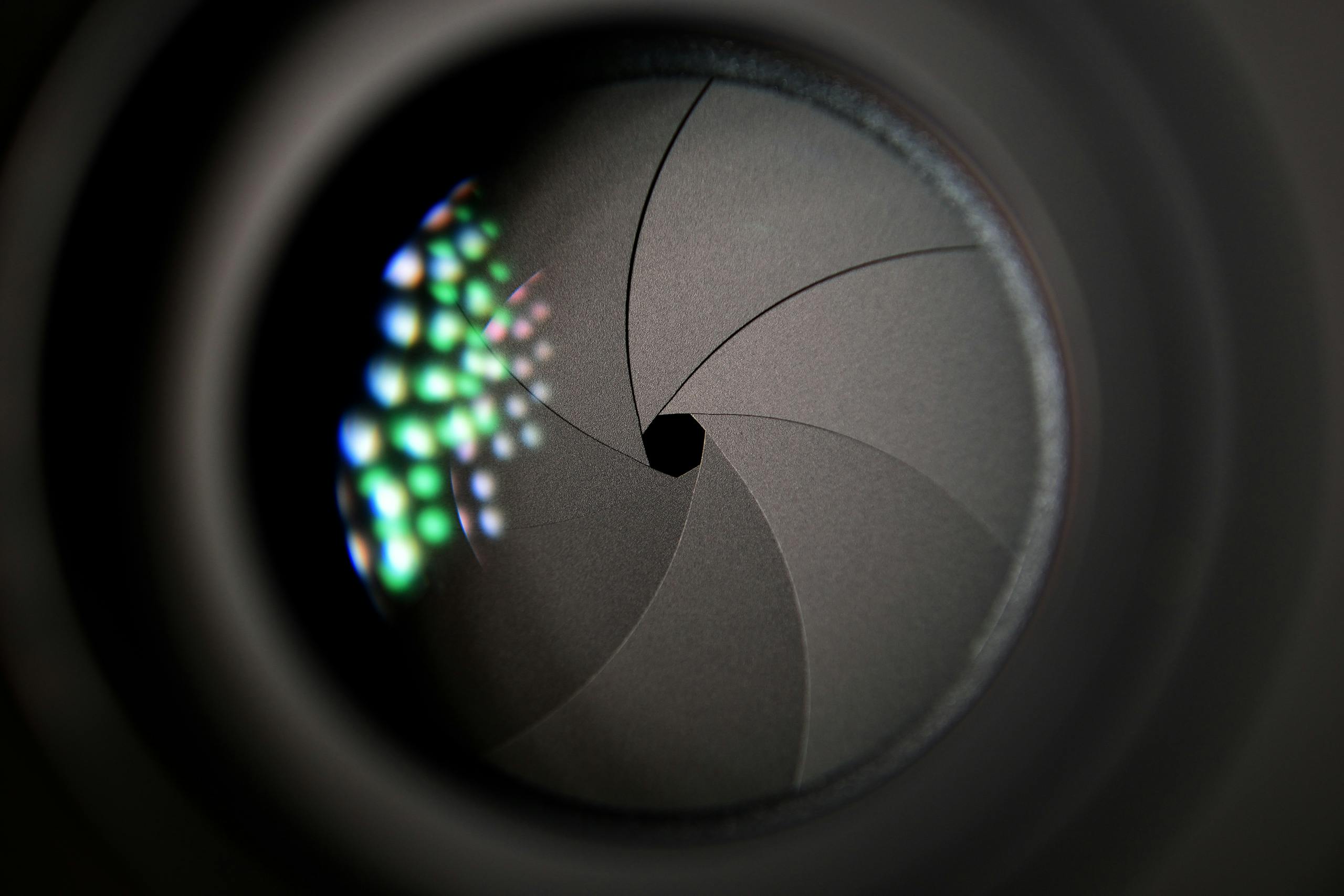
Researchers have unveiled a new design for multilayer metalenses that could make cameras in smartphones, drones, and even satellites thinner, lighter, and more powerful. This breakthrough overcomes long-standing physical limits in lens design, potentially opening the door to compact, multicolor optical systems that traditional glass lenses cannot achieve.
What Exactly Are Metalenses?
Before diving into the new development, it helps to understand what metalenses are. Unlike traditional lenses made from curved glass, metalenses are ultrathin optical devices created from arrays of nanoscale structures, sometimes just a fraction of the width of a human hair. These structures manipulate light at the subwavelength scale, bending and focusing it in ways that bulky curved glass cannot.
Metalenses have a number of advantages:
- They can be much thinner and lighter than traditional lenses.
- They can be engineered to control light in unconventional ways.
- Their features can enable focal lengths or optical effects not possible with standard designs.
The major challenge, however, has been building a metalens that works for multiple wavelengths of light—in other words, a multicolor lens. That’s where the latest research comes in.
Why Single-Layer Metalenses Fall Short
The new work highlights the physical limitations of single-layer metalenses. When researchers tried to focus multiple wavelengths of light using just one layer of nanostructures, they ran into a problem:
- A single metasurface layer can only achieve a limited group delay (the ability to delay different parts of a light wavefront to bring them into focus).
- That limitation sets hard bounds on the product of three things: the numerical aperture (NA), the lens diameter, and the bandwidth of operation.
In simpler terms, if you try to make a single-layer metalens that can focus a broad range of colors, you’re forced to compromise either by shrinking the lens size or reducing the NA so much that it barely focuses light. This trade-off makes broadband, large-aperture single-layer metalenses impractical.
The Multilayer Solution
To overcome these limits, the researchers—led by Joshua Jordaan at the Australian National University in collaboration with Friedrich Schiller University Jena—developed a multilayer metalens architecture.
Here’s how it works:
- Each layer in the stack is designed to focus a specific wavelength (or narrow band).
- Off-resonance, the layer has minimal effect on other wavelengths, reducing interference.
- By stacking multiple layers, the team spread the burden of controlling different colors across the structure.
This approach decouples the wavelength management, making the whole system more efficient and removing the strict trade-offs of a single layer. The layers are separated just enough to avoid strong interlayer coupling, which also makes the design more tolerant to fabrication misalignments.
Designing the Nanostructures
A big part of the success came from using an inverse design algorithm. Instead of manually designing nanoscale shapes, the researchers let a computational process search for geometries that would produce the required optical behavior.
Key features of the design strategy:
- They parameterized the meta-atom shapes flexibly but enforced rotational symmetry, which ensured polarization insensitivity.
- The algorithm identified nanostructures that could produce overlapping electric and magnetic dipole resonances—known as Huygens resonances—at target wavelengths.
- These resonances enabled highly efficient wavefront shaping for each layer.
The algorithm didn’t just spit out simple circles or squares. Instead, it produced a library of tiny, unexpected shapes: rounded squares, four-leaf clovers, propellers, and more. Each structure was about 300 nanometers tall and 1000 nanometers wide, small enough to manipulate light directly at the nanoscale.
The full library covered the entire 0 to 2π phase shift range, meaning the researchers could map arbitrary phase gradients across the lens surface. This is the equivalent of being able to program the focusing power of the lens at will.
Simulation Results and Performance
To test their design, the team simulated a dual-wavelength metalens operating in the near-infrared (NIR) range:
- Target wavelengths: 2000 nm and 2340 nm.
- Numerical aperture (NA): about 0.11.
The results were impressive:
- The lens achieved nearly diffraction-limited focusing.
- At 2000 nm, the focusing efficiency was about 65%.
- At 2340 nm, the efficiency was about 56%.
- Compared to an ideal lens of the same size, those numbers corresponded to 76% and 65% relative efficiency.
For an early proof-of-concept, those numbers are promising—especially considering that the design is scalable and relatively tolerant of fabrication errors.
Manufacturing Advantages
The researchers emphasized several features that make the multilayer metalens practical for real devices:
- Low aspect ratio: Each layer is thin relative to its width, making it easier to fabricate.
- Independent fabrication: Layers can be fabricated separately and later packaged together.
- Scalable fabrication methods: The design is compatible with existing semiconductor nanofabrication platforms, making industrial scaling more realistic.
- Error tolerance: The polarization insensitivity and interlayer decoupling reduce sensitivity to small fabrication defects.
This combination of design efficiency and manufacturing practicality means multilayer metalenses may not remain confined to lab experiments—they could actually find their way into consumer and industrial technology.
Limits of the Multilayer Approach
While the new design solves major issues, it isn’t without constraints:
- In practice, the multilayer system is limited to about five different wavelengths.
- Beyond that, structures resonant at long wavelengths become too large, and shorter wavelengths risk unwanted diffraction or interference.
So while it’s not yet a universal solution for fully broadband lenses, it’s a huge step forward compared to what single-layer metasurfaces can offer.
Real-World Applications
The team highlighted several potential uses for this technology:
- Smartphone cameras: Metalenses could replace bulky glass lenses, creating thinner, lighter devices with high-quality imaging.
- Drones: Small flying platforms where weight is critical would benefit from ultralight optical systems.
- Earth-observation satellites: In space, every gram matters. Compact, high-performance lenses could make imaging satellites lighter and cheaper to launch.
In all these cases, the ability to focus multiple colors of light with a thin, lightweight device could significantly expand the capabilities of portable imaging systems.
Adding Context: Why Multicolor Lenses Matter
To appreciate why this matters, think about everyday cameras. Whether in your phone or in professional equipment, a camera needs to focus multiple colors (red, green, blue, etc.) at once. Traditional lenses handle this with stacks of curved glass elements, carefully shaped and layered to correct for chromatic aberration.
Metalenses, until now, haven’t been able to match that multicolor performance, especially at practical sizes. This research demonstrates a clear path forward: thin, stacked metasurfaces that mimic the role of glass lens stacks but in an ultracompact form.
A Closer Look: What Are Huygens’ Metasurfaces?
The term Huygens’ metasurface refers to a special class of metasurfaces that balance electric and magnetic dipole resonances to achieve complete control over light transmission with minimal reflection.
- When electric and magnetic responses overlap, the metasurface can steer or shape wavefronts very efficiently.
- This principle allows for high transmission efficiency and flexible wavefront engineering.
- In practice, Huygens’ metasurfaces are an ideal building block for metalenses.
The researchers took advantage of this concept by designing their nanostructures specifically to achieve these resonances.
Future Directions
The current proof-of-concept focused on the near-infrared range, but the principles can extend to visible light as fabrication technology advances. Challenges remain, particularly in scaling down the structures for shorter wavelengths without losing efficiency.
Still, the combination of inverse design methods, multilayer stacking, and semiconductor-ready fabrication suggests that practical, mass-produced multicolor metalenses are closer than ever.
Why This Research Stands Out
Metasurfaces have been a hot topic in optics for more than a decade, but most designs have struggled to move beyond lab demonstrations. The new multilayer approach stands out because it is:
- Grounded in realistic manufacturing techniques.
- Directly aimed at solving real problems like multicolor focusing, size, and scalability.
- Tested with practical performance metrics like diffraction-limited focusing and efficiency.
If developed further, this could be one of the first metalens technologies to see mainstream adoption.
Reference
Research paper: Design of multilayer Huygens’ metasurfaces for large-area multiwavelength and polarization-insensitive metalenses (Optics Express, 2025)


