A New Dimension for Quantum Sensing as Researchers Create 2D Spin Qubits in Diamond
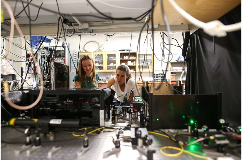
The quest for practical quantum technologies just got a major boost thanks to researchers at the University of California, Santa Barbara (UCSB). Working at the intersection of materials science and quantum physics, the lab led by Professor Ania Jayich, co-director of UCSB’s National Science Foundation Quantum Foundry, has achieved something extraordinary—creating two-dimensional ensembles of interacting spin qubits inside diamond.
This achievement, led by Ph.D. graduate Lillian Hughes, marks the first time scientists have demonstrated a strongly interacting, two-dimensional, dipolar spin ensemble in diamond. The results, published across three major papers—one in Physical Review X (PRX) and two in Nature in 2025—show that these specially engineered diamonds can enable new kinds of entanglement-assisted quantum sensing with potential metrological advantages far beyond classical limits.
How the Researchers Built a New Kind of Diamond Qubit System
The foundation of this research lies in nitrogen-vacancy (NV) centers, which are small defects inside diamond crystals. An NV center forms when one carbon atom in the lattice is replaced by a nitrogen atom, leaving an empty spot next to it—a vacancy. This defect traps an electron whose spin behaves like a tiny magnet. That spin can be manipulated and measured, giving the NV center its remarkable ability to act as a quantum sensor.
NV centers have been used in sensing since the 2000s because their spin states are stable even at room temperature. But until now, most experiments involved single spins or ensembles of non-interacting spins, which limited their potential.
Hughes and her colleagues took a new approach: instead of studying isolated NV centers, they designed a dense, planar layer of NV defects inside lab-grown diamond. Using plasma-enhanced chemical vapor deposition (PECVD), they grew the diamond on a (111)-oriented substrate, which allows NV centers to align in a way that promotes non-zero dipolar interactions—meaning the spins actually influence each other rather than acting independently.
This change in orientation may sound small, but it’s a big deal. In standard (001) diamond, the dipolar interactions often cancel out due to symmetry. By switching to (111), the UCSB team created conditions for strong spin coupling, essential for quantum entanglement and collective quantum behavior.
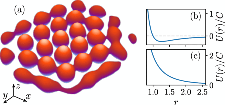
Their PRX paper, titled “Strongly Interacting, Two-Dimensional, Dipolar Spin Ensembles in (111)-Oriented Diamond,” describes how this unique configuration produces a dense 2D layer of NV centers confined just below the diamond surface. Each NV center interacts with its neighbors through dipolar forces, forming a quantum-connected layer of spins—a true 2D quantum material inside a solid crystal.
Why This Discovery Matters
This breakthrough matters because it changes the way quantum sensing can be done. Traditional sensors, whether optical or magnetic, are limited by what’s called the standard quantum limit, which scales with the square root of the number of particles, N. That means doubling the number of sensors only improves precision by about 40%.
However, when quantum particles become entangled, their collective behavior allows for sensitivities that surpass this limit—a phenomenon known as quantum metrological advantage. The UCSB team has shown that by using interacting NV centers in diamond, it’s possible to break the standard quantum limit, bringing real-world quantum advantage closer to reality.
This advance also has practical implications. Solid-state quantum sensors, like those made from diamond, can operate at room temperature and can be positioned extremely close to samples—such as biological tissues, new materials, or superconductors—without the need for bulky vacuum chambers or cooling systems. That makes them ideal for exploring magnetic, electronic, or biological phenomena at the nanoscale.
Two Ways to Boost Quantum Measurements
In addition to the PRX paper, the UCSB team published two companion studies in Nature, each revealing a different route to improved measurement precision using the same diamond spin ensemble.
- Signal Amplification via Many-Body Echoes
In one paper, the researchers demonstrated signal amplification in a solid-state sensor using a technique called asymmetric many-body echo. By engineering the way spins interact and then partially reversing those interactions, they managed to amplify magnetic signals without increasing the noise. The system effectively magnifies weak signals, making them easier to detect—similar to zooming in on a faint image until the details become visible. The study reports measurable signal amplification of around 6.7%, achieved at room temperature, showing how collective spin interactions can be harnessed to boost performance beyond classical methods. - Spin Squeezing for Noise Reduction
The second Nature paper demonstrated spin squeezing—a quantum process that redistributes uncertainty between different components of the spin system to reduce noise in the measurement direction. By doing this, they effectively “squeeze” the quantum noise, achieving finer precision in their readings. The UCSB group observed −0.50 ± 0.13 dB of spin squeezing, representing the first demonstration of this phenomenon in a solid-state NV ensemble at room temperature. It’s a small but crucial proof that solid-state qubits can achieve correlated states suitable for quantum-enhanced metrology.
Together, these studies show two complementary paths to better quantum measurements: amplifying the signal and suppressing the noise. Both effects are vital for practical quantum sensors that could outperform existing technologies.
The Engineering Challenge Ahead
While these results are remarkable, the researchers acknowledge that several technical challenges remain. One key goal is to precisely control the positions of NV centers within the 2D plane. Right now, the defects are created somewhat randomly during growth. To reach full quantum advantage, scientists need to arrange them into regular grids, spacing each qubit at a specific distance to optimize coupling and minimize unwanted interactions.
There’s also the issue of decoherence—the tendency for quantum states to lose coherence over time due to environmental disturbances. Though NV centers are among the most robust qubits known, maintaining coherence in dense, interacting systems requires careful material engineering and magnetic shielding.
Still, Jayich’s lab believes these obstacles are surmountable. Their approach—combining precision materials science with advanced quantum control—positions diamond as a leading platform for solid-state quantum sensing.
Why Diamond Is So Special for Quantum Science
Diamonds have become the poster child of quantum materials, and for good reason. Unlike most qubit systems that require cryogenic temperatures, NV centers in diamond can operate at room temperature and maintain long spin coherence times (milliseconds or more). They can also be optically addressed, meaning lasers can initialize and read out their quantum states directly.
Moreover, diamond’s chemical stability makes it a fantastic host for quantum defects. Scientists can bring samples—like proteins, magnetic materials, or thin films—within nanometers of the NV layer, enabling nanoscale magnetic imaging and single-molecule spectroscopy.
This accessibility is what makes NV-based sensors so promising for applications ranging from medical imaging and brain studies to superconductivity research and next-generation electronics.
The UCSB research pushes these possibilities further by making NV centers not just passive sensors but interacting quantum systems capable of collective behavior. This is an essential step toward quantum-enhanced devices that operate reliably under real-world conditions.
The Future of Quantum Sensing
Looking ahead, the next milestones involve scaling up these systems and refining control. If researchers can create ordered arrays of NV centers in diamond, they could simulate quantum many-body physics or perform high-resolution magnetic field mapping with unprecedented sensitivity.
Beyond sensing, the same principles could inform the design of quantum simulators or even hybrid quantum computers where ensembles of spins act as robust quantum registers.
The materials challenge—placing spins at defined positions in the diamond lattice—remains a major focus for Jayich’s team. As Hughes moves to continue her research at Caltech, this work will likely expand, with collaborations between quantum engineers, material scientists, and theorists all contributing to the next phase of diamond-based quantum technology.
In the near term, the UCSB team expects to demonstrate a useful quantum advantage in sensing applications—showing not just a theoretical improvement but a measurable one that outperforms the best classical sensors available today.
That would be a fitting payoff for years of careful diamond engineering, creative physics, and the persistence of researchers determined to push quantum science from the lab into everyday tools.
Research References:
- Lillian B. Hughes et al., Strongly Interacting, Two-Dimensional, Dipolar Spin Ensembles in (111)-Oriented Diamond, Physical Review X (2025). https://doi.org/10.1103/PhysRevX.15.021035
- Haoyang Gao et al., Signal Amplification in a Solid-State Sensor Through Asymmetric Many-Body Echo, Nature (2025). https://doi.org/10.1038/s41586-025-09452-7
- Weijie Wu et al., Spin Squeezing in an Ensemble of Nitrogen–Vacancy Centres in Diamond, Nature (2025). https://doi.org/10.1038/s41586-025-09524-8
