Hidden Cavities in 2D Devices Could Revolutionize Quantum Materials Research
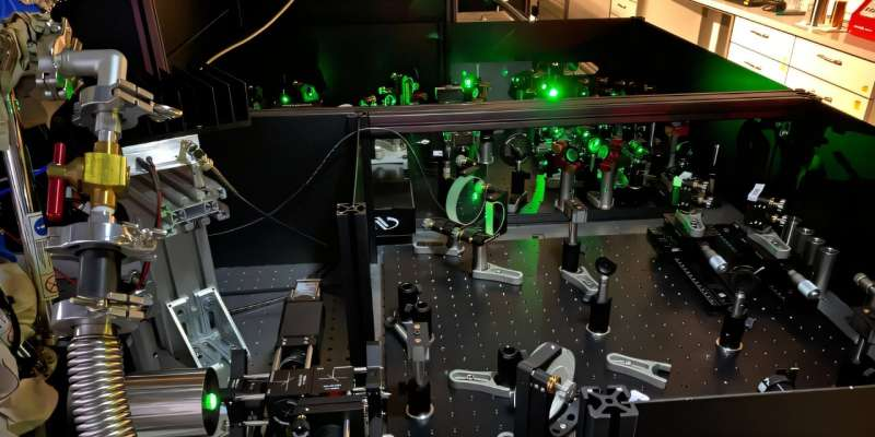
Scientists have made a fascinating discovery about two-dimensional (2D) materials—those incredibly thin layers just a few atoms thick that have been exciting physicists for over a decade. A team led by Columbia University and the Max Planck Institute for the Structure and Dynamics of Matter (MPSD) has found that when these materials are stacked together in tiny devices, they can naturally form hidden cavities—microscopic spaces that trap light and electrons.
These cavities, it turns out, can drastically alter how electrons behave. The team’s experiments reveal that these hidden spaces can confine terahertz light (THz)—a type of radiation between microwaves and infrared light—and interact with the electrons in ways that could explain some of the mysterious quantum behaviors observed in 2D materials.
Their results, published in Nature Physics in October 2025, open an unexpected new way to control and manipulate quantum phases—the unusual electronic states that make 2D materials such a rich field for research.
What Makes 2D Materials So Interesting
2D materials are crystalline sheets that are only one atom thick, with graphene being the most famous example. When stacked or combined, they can form what are called van der Waals heterostructures—layered systems where each layer brings its own electronic and optical properties.
Researchers love these systems because they can host quantum phases such as superconductivity, exotic magnetism, and correlated insulating states. But one big challenge remains: why and how these phases emerge, and how to control them precisely.
That’s where light—especially terahertz radiation—comes in. Terahertz frequencies correspond to energy scales of a few millielectronvolts, which happen to be the same range where many of these quantum effects occur. Probing 2D materials at these frequencies could reveal how their electrons move and interact—but it’s not an easy task.
A key problem is scale mismatch. The wavelengths of terahertz light (around 1 millimeter) are much larger than the size of 2D devices (a few micrometers). Imagine trying to use a one-meter-long ruler to measure the details of a single hair. That’s how hard it is to use normal optical techniques to study these tiny systems.
Building a Miniature Spectroscope
To overcome this, the researchers built a chip-scale terahertz spectroscope. This tiny instrument confines terahertz light within microscopic circuits, shrinking the wavelength down from 1 millimeter to about 3 micrometers. This allows the team to directly visualize how light and electrons behave inside 2D devices.
They started by testing their setup on graphene, since its electronic properties are already well understood. By shining green ultrafast laser pulses onto the sample inside a cryostat (a chamber cooled to cryogenic temperatures), they generated and detected the terahertz light.
What they found surprised them. Instead of a simple, uniform response, the device produced standing waves—patterns that form when waves reflect and interfere with themselves, much like the vibrations on a guitar string.
Discovering Hidden Cavities
Here’s where the discovery gets really interesting. In ordinary optics, standing waves can form when light bounces between two mirrors, creating what’s called a cavity. Cavities are fundamental in optics and quantum physics—they allow light and matter to interact strongly, leading to phenomena like cavity electrodynamics and polariton formation.
But in this case, there were no mirrors. The 2D device itself—just a few stacked layers—was acting as the cavity.
The edges of the conducting layers, it turns out, naturally reflect terahertz waves, creating confined self-cavity modes. These modes trap light and electrons together, forming hybrid quasiparticles known as plasmon polaritons—waves that are part light, part electron oscillation.
The researchers realized that each layer in the structure—graphene, graphite gates, and the dielectric layers between them—can act as its own tiny cavity, separated by only tens of nanometers. These cavities can then interact with each other, just like connected guitar strings influence each other’s tone. When the coupling is strong enough, it enters what physicists call the ultrastrong coupling regime, where the interaction energy between light and matter becomes comparable to the frequency of the light itself.
In this regime, the properties of the material can change dramatically.
Hybrid Light–Matter Behavior
By tuning the carrier density (the number of electrons) in the graphene layer, the researchers could control the frequency of the plasmons—the oscillations of electrons. When these plasmon frequencies matched the natural resonance of the self-cavity modes, they saw clear signs of hybridization.
In simple terms, the plasmons and cavity photons mixed together to form new hybrid modes with frequencies and properties that could not exist independently.
The data matched beautifully with an analytical theory developed by the team, led by MPSD postdoctoral researcher Marios Michael. The model needed only a few parameters—the geometry of the sample, dielectric properties, and layer thickness—to reproduce the observations.
This theoretical tool, combined with the spectroscope, now allows scientists to extract the key properties of 2D materials automatically. By analyzing how the resonances change with temperature, carrier density, or magnetic field, researchers can uncover the mechanisms that drive different quantum phases.
Implications for Quantum Materials
This discovery adds a completely new layer of control in the study of quantum materials. If cavities can form naturally inside 2D devices, they can enhance or suppress interactions between light and matter in ways that were previously hidden.
It also means that many earlier experiments on 2D materials—especially those studying optical and electronic properties—might have unknowingly been influenced by these cavity effects. Understanding this could help re-interpret past data and design better experiments in the future.
Even more exciting is the potential to engineer these cavities intentionally. By designing the geometry of the device—the width, gate configuration, or dielectric environment—scientists could create devices with tailored light–matter coupling. This could allow precise tuning of superconductivity, magnetism, or charge order in these quantum systems.
Beyond Graphene: Expanding the Technique
Although this initial study focused on graphene and graphite gates, the researchers say their chip-scale terahertz spectroscope can be used on a wide range of materials.
Many other 2D systems—like transition metal dichalcogenides (TMDs), twisted bilayer graphene, or heterostructures with moiré patterns—are known to host rich quantum behavior. The new technique can reveal how self-cavity effects might influence superconductivity, charge density waves, or excitonic insulators in those materials.
The team is already applying their approach to new samples, both in Hamburg and at Columbia University, to see how universal these cavity effects are.
Understanding Cavity Electrodynamics
To put this in context, cavity electrodynamics is the study of how light interacts with matter in confined spaces. When light is trapped between mirrors—or in this case, within the natural boundaries of a 2D device—it can enhance the electromagnetic field intensity by orders of magnitude.
This enhanced field leads to stronger coupling between photons and electrons, resulting in hybrid light–matter states. In extreme cases, it can even modify the fundamental properties of the material—changing its conductivity, magnetism, or superconductivity.
In the ultrastrong coupling regime, the interaction energy becomes comparable to the photon energy itself. This means that even the vacuum fluctuations—the tiny electromagnetic ripples that exist in empty space—can start influencing the ground state of the system.
That’s a mind-bending concept: the mere presence of a confined electromagnetic field could alter the material’s intrinsic properties.
What Are Plasmon Polaritons?
A key player in this study is the plasmon polariton—a hybrid wave that combines oscillations of free electrons (plasmons) with light waves (photons).
In metals and conductive 2D materials, electrons can collectively oscillate at certain frequencies, creating plasmons. When these couple with light, they form plasmon polaritons, which can travel along surfaces or interfaces.
Because they are confined to very small dimensions—often much smaller than the wavelength of light—plasmon polaritons allow scientists to focus electromagnetic energy far beyond the limits of conventional optics.
This makes them powerful tools for exploring nanoscale phenomena, sensing, and even developing components for quantum information technology.
A Serendipitous Discovery
Interestingly, this breakthrough wasn’t part of the original plan. The researchers were mainly testing how well their new spectroscope could measure the optical conductivity of graphene. The self-cavity modes appeared unexpectedly during their measurements.
Realizing what they had stumbled upon, they expanded their analysis and confirmed the cavity effects both experimentally and theoretically.
What began as a routine measurement turned into the discovery of an entirely new physical effect—one that might redefine how scientists understand light–matter interactions in 2D materials.
Looking Ahead
The findings mark a significant step forward in understanding how geometry and light confinement shape the behavior of quantum materials. It bridges the fields of condensed matter physics and cavity quantum electrodynamics, two areas that rarely overlap at the nanoscale.
As research continues, scientists hope to explore how these self-cavities might be used to stabilize or even induce new quantum phases, leading to breakthroughs in quantum computing, sensors, and next-generation electronic devices.
The next time physicists observe unusual electronic behavior in a 2D material, they’ll have to consider an intriguing new question: Could hidden cavities be playing a part?
Research Reference:
Cavity electrodynamics of van der Waals heterostructures – Nature Physics (2025)

