Hybrid Metasurface Breakthrough: Low-Voltage Light Modulation for Energy-Efficient Optics
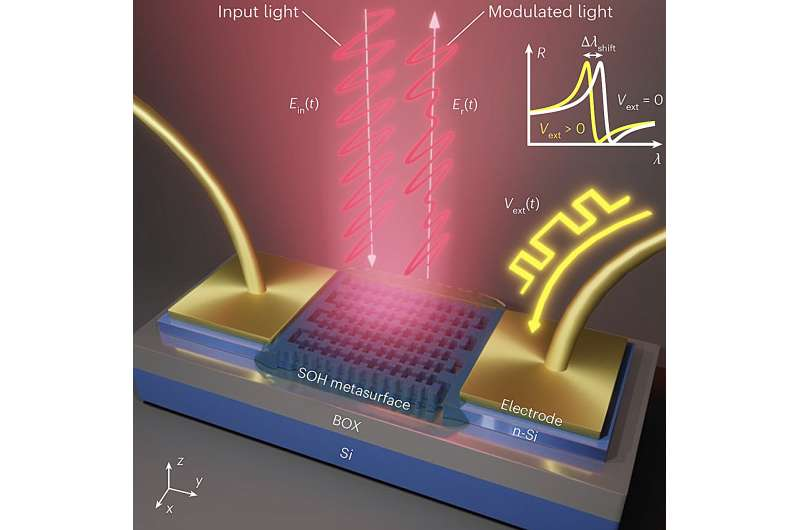
Researchers at The University of Tokyo have unveiled a new type of hybrid electro-optic metasurface that could dramatically change how we control light in optical systems. The innovation, published in Nature Nanotechnology (2025), achieves high-speed light modulation using voltages as low as 0.2 volts—a remarkable leap toward low-power, high-efficiency optical communication and computing technologies.
This study, titled “Subvolt high-speed free-space modulator with electro-optic metasurface”, represents a major milestone in active metasurface design. These devices are among the most promising technologies for next-generation photonics, and this research tackles one of their biggest limitations: high power consumption.
What Are Metasurfaces and Why They Matter
To understand why this is such a big deal, it helps to know what metasurfaces are. Essentially, a metasurface is a two-dimensional (2D) array of nanoscale structures—tiny patterns etched or printed on a surface that can manipulate light in ways natural materials can’t. By engineering these patterns carefully, scientists can control light’s phase, amplitude, polarization, and even its direction.
They’re incredibly thin (often just a few hundred nanometers thick), and they can perform optical functions that would otherwise require bulky components like lenses or prisms. This makes them a key technology in compact photonics, AR/VR systems, beam steering, and optical communications.
An active metasurface goes a step further. Instead of having a fixed optical behavior, its properties can be tuned in real-time using electrical signals. This enables dynamic modulation—changing how the metasurface interacts with light at high speed. Such functionality is essential for applications like optical data transmission, adaptive sensing, and programmable optics.
However, most active metasurfaces developed so far require high operating voltages (often tens of volts) to achieve meaningful modulation. That makes them power-hungry and less practical for integration with existing electronic systems, especially those based on CMOS (Complementary Metal–Oxide–Semiconductor) technology, which is standard in modern electronics.
The Tokyo Team’s Low-Voltage Metasurface
The new metasurface developed by Go Soma, Koto Ariu, Seidai Karakida, Yusuke Tsubai, and Takuo Tanemura from The University of Tokyo changes this narrative completely. Their approach combines silicon nanostructures with an organic electro-optic (OEO) layer to create a silicon–organic hybrid (SOH) device capable of modulating light at sub-volt levels.
In essence, it’s a hybrid between traditional semiconductor technology (silicon) and advanced organic materials that respond strongly to electric fields. This combination is key to achieving both low driving voltage and high-speed performance.
What’s more impressive is that the fabrication process is compatible with standard CMOS manufacturing, meaning this device could eventually be produced using the same industrial techniques already used to make computer chips. That compatibility is a huge advantage—it brings this technology closer to real-world applications and large-scale integration.
How the Device Works
At the heart of the design lies a clever nanostructure geometry known as a dimerized grating. Imagine a regular array of silicon bars—but instead of all bars being identical, two slightly different widths alternate. This breaks the symmetry of the structure and enables a special optical resonance called a quasi-bound state in the continuum (q-BIC).
This resonance allows light to be trapped and concentrated within the metasurface for a longer time than usual. The trapped light interacts strongly with the organic electro-optic material that fills tiny gaps (slots) in the silicon structure.
Because of this tight confinement of both the optical and electrical fields, even a small change in voltage can produce a large change in optical response. In other words, the device achieves strong modulation with very little power.
In simple terms: light gets squeezed into an extremely small volume, overlaps perfectly with the electric field, and the organic material quickly responds to even a tiny voltage change—leading to efficient light modulation.
Performance Results
The researchers demonstrated that their metasurface could achieve data transmission at 50 megabits per second (Mbps) using only 0.2 volts, and at 1.6 gigabits per second (Gbps) with just 1 volt.
These figures are stunning when compared to existing metasurface modulators, which typically require voltages exceeding 10 volts to reach similar performance levels. The fact that the new device operates comfortably within CMOS voltage ranges means it can be directly integrated with standard electronic drivers without special amplifiers.
They also demonstrated that their metasurface can operate as a free-space optical modulator, meaning it doesn’t need fiber coupling—it works directly with beams of light in air. That’s especially promising for free-space optical communication systems, where light carries data between points without physical connections, such as satellite-to-satellite links or inter-chip communications.
The team’s smaller test device, around 10 square micrometers, achieved a modulation bandwidth of about 0.38 GHz (380 MHz). Using pulse-amplitude modulation (PAM4), they successfully transmitted data at 1.6 Gbps—impressive numbers for such a tiny, low-power device.
Why This Matters
Optical modulators are the backbone of modern communication systems. They convert electronic data into light signals that can travel through optical fibers or free space. Making these modulators smaller, faster, and more power-efficient is crucial for the next wave of technologies—ranging from 5G/6G networks and quantum communication to AI accelerators that use light for computation.
Until now, metasurface-based optical modulators have remained largely experimental because they required large driving voltages and complex fabrication. This new approach could change that by enabling sub-volt operation at high speed, all while staying compatible with industry-standard silicon processes.
The work also opens doors for energy-efficient optical computing, where photons replace electrons for data processing. Since optical signals don’t generate heat the same way electrical currents do, devices like this metasurface could make future computers faster and more sustainable.
The Science Behind the Innovation
A few core principles make this achievement possible:
- High-Q Resonance – The dimerized grating design supports a resonance with a very high quality factor (Q). This means light stays trapped within the structure for longer, amplifying its interaction with the material.
- Slot Confinement – The device’s nanostructure confines light into ultra-narrow slots filled with the electro-optic material. This overlapping of electric and optical fields maximizes modulation efficiency.
- Organic Electro-Optic Layer – The organic material used has strong electro-optic coefficients, meaning it changes its refractive index quickly in response to small voltage changes.
- CMOS Compatibility – By basing the design on silicon and processes already used in semiconductor fabrication, the metasurface can be more easily integrated into electronic circuits and scaled for production.
Together, these design choices create a sub-volt, high-speed modulator—something long sought after in photonics research.
Potential Applications
This hybrid metasurface technology could impact several areas:
- Free-space optical communication – Low-voltage, high-speed light modulators can transmit data wirelessly at optical frequencies, offering faster and more secure links than traditional radio systems.
- Beam steering and LiDAR – Tunable metasurfaces can dynamically redirect light beams, enabling compact and efficient LiDAR systems for autonomous vehicles or drones.
- Optical computing – Fast light modulation at low power could make all-optical logic circuits more feasible, supporting data centers or AI processors that use photonic architectures.
- Sensing and imaging – Dynamic metasurfaces could act as adaptive lenses or sensors, adjusting their optical properties in real time for better precision.
Because the new design operates at voltages compatible with existing chips, it could be integrated into future electronic-photonic systems without extensive redesigns.
Limitations and Next Steps
While the results are extremely promising, this is still a lab-scale demonstration. The device’s speed—while impressive at around 1.6 Gbps—is still far below the tens of gigabits per second achievable by commercial fiber-optic modulators. However, the potential for improvement is significant.
Future research will likely focus on:
- Scaling the technology to larger arrays for higher modulation speeds.
- Enhancing the bandwidth through improved nanostructure design.
- Improving durability of the organic materials used, which can be sensitive to heat or environmental factors.
- Exploring phase modulation, not just intensity modulation, for broader optical communication use.
Even with these challenges, the ability to modulate light at sub-volt levels marks a huge stride toward energy-efficient optical devices. It bridges the gap between conventional electronics and high-speed photonics.
Broader Context: The Rise of Active Metasurfaces
Metasurfaces are one of the fastest-evolving areas in optics today. They’re already being explored for flat lenses, holographic displays, polarization control, and quantum photonics. The transition from passive to active metasurfaces—those that can be electrically or optically controlled—is what truly unlocks their potential.
In recent years, different strategies have been explored for tunable metasurfaces:
- Phase-change materials (like GST) that change optical properties with temperature.
- Liquid crystals controlled by electric fields.
- MEMS (micro-electro-mechanical systems) that physically move parts of the surface.
- Graphene or TCO-based layers that change conductivity with voltage.
Each approach has trade-offs in speed, voltage, and fabrication complexity. What makes the Tokyo team’s hybrid approach stand out is that it balances all three—achieving high speed, low voltage, and standard fabrication compatibility in one device.
This hybrid concept could also inspire similar combinations of semiconductors and organic materials to make new classes of tunable optical components.
Looking Ahead
The idea of controlling light using voltages as small as a fraction of a volt is revolutionary. It means optical systems could soon be powered and driven as easily as today’s electronic circuits. That could redefine how we design everything from data centers to wearable sensors.
If the technology scales successfully, we might see metasurface modulators integrated directly into chips, forming ultra-fast optical interconnects or compact imaging systems that consume minimal power.
In the grand picture, innovations like this bring us closer to merging photonics with electronics—a long-standing goal in science and engineering that promises faster, more efficient, and more compact devices.
Research Reference:
Go Soma, Koto Ariu, Seidai Karakida, Yusuke Tsubai & Takuo Tanemura (2025). Subvolt high-speed free-space modulator with electro-optic metasurface. Nature Nanotechnology. https://doi.org/10.1038/s41565-025-02000-4
