LLNL and Stanford Break 3D Nanofabrication Barriers with Meta-Optics and Ultra-Fast Two-Photon Lithography
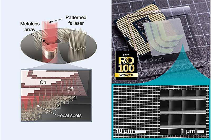
Researchers at Lawrence Livermore National Laboratory (LLNL), working closely with Stanford University, have achieved a major leap forward in 3D nanofabrication, turning what was once a slow, lab-bound technique into a process that could realistically support wafer-scale manufacturing. Their work, published in Nature on December 17, introduces a new platform that dramatically expands the speed, scale, and flexibility of two-photon lithography (TPL) without sacrificing its defining advantage: submicron precision.
At the heart of this advance is a clever fusion of meta-optics and adaptive light control, allowing researchers to reshape how light itself is used to build materials at the nanoscale. The platform, now known as MetaLitho3D, has already earned a 2025 R&D 100 Award, signaling strong interest beyond academic research and into potential industrial adoption.
Why Two-Photon Lithography Needed a Rethink
Two-photon lithography has long been admired for its ability to create highly intricate 3D structures with features well below one micrometer. It works by focusing ultrafast laser pulses into a photosensitive material, where polymerization occurs only at the exact focal point. This gives TPL exceptional spatial control and resolution.
However, the technique has always come with a serious limitation. Traditional TPL systems rely on microscope objectives, which restrict the printable area to a field of view measured in hundreds of microns. To fabricate anything larger, researchers must stitch together thousands of tiny tiles, a process that is not only slow but also prone to alignment errors. These constraints have kept TPL largely confined to research labs, preventing it from becoming a practical manufacturing tool.
The LLNL–Stanford team set out to solve this fundamental bottleneck.
Replacing a Single Lens with Thousands of Metalenses
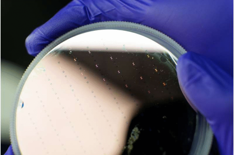
The key innovation behind MetaLitho3D is the replacement of the traditional microscope objective with large arrays of metalenses. Metalenses are engineered, ultrathin optical elements that can precisely shape and focus light using nanostructured surfaces rather than bulky curved glass.
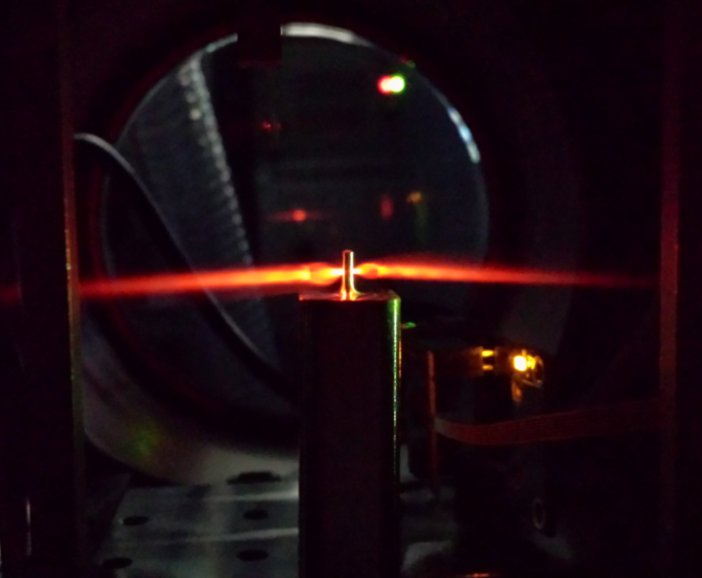
In this system, a femtosecond laser is split into more than 120,000 coordinated focal spots using tiled arrays of high–numerical-aperture metalenses. Each metalens effectively acts as a miniature printer, writing its own region of the structure. Instead of scanning a single beam across the material, the system prints thousands of regions in parallel, all in a single pass.
This massively parallel approach allows the platform to write across centimeter-scale areas while maintaining a minimum feature size of just 113 nanometers. Even more striking is the speed: the team reports throughput more than a thousand times faster than that of commercial TPL systems.
By spacing focal spots according to the metalens pitch rather than crowding them into a tiny optical field, the researchers also avoided the proximity effects that had plagued earlier multi-beam attempts.
Adaptive Meta-Lithography and Real-Time Light Control
While the metalens arrays alone are impressive, the system’s capabilities expand even further through the integration of a spatial light modulator (SLM). This device enables real-time, independent control of each focal spot’s intensity, allowing beams to be switched on or off, fine-tuned with grayscale modulation, and coordinated dynamically during printing.
Initially introduced to equalize beam intensity across the array, this adaptive control quickly revealed much broader possibilities. The team realized they could fabricate non-periodic and fully stochastic structures while still retaining high levels of parallelization.
This adaptive approach, formally named Adaptive Meta-Lithography, allows for precise control over linewidths, layer-by-layer patterning, and selective exposure across the print area. In one demonstration, the researchers produced 16 different microscopic chess openings in a single fabrication process, highlighting both the precision and flexibility of the system.
From Laboratory Curiosity to Industrial-Scale Tool
One of the most important implications of this work is that two-photon lithography may finally be ready for industry adoption. By enabling wafer-scale nanomanufacturing, MetaLitho3D brings TPL closer to the production model used in the semiconductor industry, where extremely complex structures are manufactured in volume at low unit cost.
The ability to fabricate intricate 3D architectures at high speed opens the door to applications that were previously impractical or prohibitively expensive.
What Can Be Made with MetaLitho3D?
The platform’s combination of speed, scale, and adaptability makes it suitable for a wide range of advanced technologies. Potential applications include:
- Photonics and meta-optical devices, such as waveguides and advanced optical components
- Microelectronics, including complex interconnects and next-generation packaging
- Microfluidic systems with intricate three-dimensional channel networks
- Quantum information technologies, particularly modular architectures for trapped-ion quantum computing chips
- Fusion energy research, where precisely fabricated 3D fuel capsules are critical
- Biomedical engineering, including scaffolds and the mass production of microscopic particles
The team estimates that the system could fabricate tens of millions of micro-particles per day, highlighting just how far beyond traditional TPL this approach reaches.
A Broader Look at Meta-Optics in Manufacturing
Meta-optics, the broader field underpinning this work, is rapidly reshaping how scientists think about controlling light. Unlike conventional optics, which rely on bulky lenses and mirrors, meta-optical components achieve their effects through carefully designed nanostructures that interact with light at subwavelength scales.
This allows optical systems to become thinner, lighter, and more versatile, while also enabling entirely new functionalities. In the context of additive manufacturing, meta-optics offers something especially powerful: the ability to precisely sculpt light itself, turning it into an ultra-fine tool for building matter.
As higher-power lasers, larger metalens wafers, and faster spatial modulators become available, systems like MetaLitho3D are expected to grow even more capable. Researchers anticipate greater complexity, higher throughput, and broader industrial relevance in the coming years.
Why This Breakthrough Matters
This work represents more than just a faster 3D printer. It marks a shift in how nanoscale manufacturing can be approached, blending optics, materials science, and additive manufacturing into a single, scalable platform.
By overcoming the long-standing trade-off between resolution and throughput, the LLNL–Stanford team has shown that it is possible to achieve both at once. If adopted widely, this technology could redefine how future microdevices, nanomaterials, and advanced systems are designed and produced.
Research paper:
Songyun Gu et al., 3D nanolithography with metalens arrays and spatially adaptive illumination, Nature (2025).
https://doi.org/10.1038/s41586-025-09842-x

