Ultra-Thin Metalens Technology Boosts Infrared Sensors for Fire and Threat Monitoring
Researchers from the ARC Centre of Excellence for Transformative Meta-Optical Systems (TMOS) have unveiled a major leap forward in infrared sensing technology — a new ultra-thin metalens that dramatically increases the sensitivity of mid-wavelength infrared (MWIR) sensors. This innovation could transform how we detect bushfires, military threats, and other heat-based phenomena, making thermal monitoring faster, cheaper, and more scalable.
The study, led by Dr. Tuomas Haggren from the Australian National University and Dr. Wenwu Pan and Associate Professor Gilberto Umana-Membreno from the University of Western Australia (UWA), introduces a flat metasurface lens thinner than a human hair. Despite its tiny size, this lens can focus and process infrared radiation with remarkable precision—without the need for cryogenic cooling, a costly requirement in current infrared detectors.
How the Ultra-Thin Metalens Works
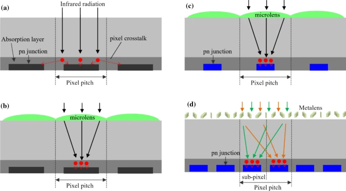
Traditional MWIR sensors rely on spherical microlenses to focus infrared light onto detector pixels. While effective, these lenses come with trade-offs. As sensor pixels get smaller to improve resolution, light tends to spill over between pixels, creating blur and reducing image sharpness. Additionally, when the detector area is increased to collect more light, it also generates more noise in the form of dark current, which occurs even when no light is present.
To reduce this noise, infrared cameras often need to be cryogenically cooled—a process that lowers the temperature of the detector to suppress unwanted electrical activity. However, this cooling system adds bulk, cost, and maintenance complexity, making it impractical for remote or large-scale applications like wildfire monitoring.
The TMOS team tackled these problems by designing an array of microscopic lenses, each about one micrometer apart, etched directly onto a thin layer known as a metasurface. These lenses—called metalenses—are made of tiny nanostructures that manipulate light in ways traditional optics cannot.
The key innovation is how the metasurface focuses infrared light precisely onto each pixel. Because every pixel gets its own mini-lens, the design both reduces light spillover and minimizes dark current, allowing the sensor to capture sharper, cleaner images.
The Science Behind the Design
The team focused on light in the 3 to 5 micrometer range, known as the mid-wavelength infrared (MWIR) band. This spectrum is ideal for detecting heat signatures, as it provides excellent thermal contrast and works effectively in both day and night conditions.
Using electromagnetic modeling and simulations, the researchers explored how to optimize the performance of the metalens array. Each lens element—or “meta-atom”—is a nanopillar smaller than the wavelength of light. By adjusting the diameter and arrangement of these pillars, the researchers achieved the desired phase shift in the incoming light waves, effectively bending and focusing them just like a traditional curved lens would.
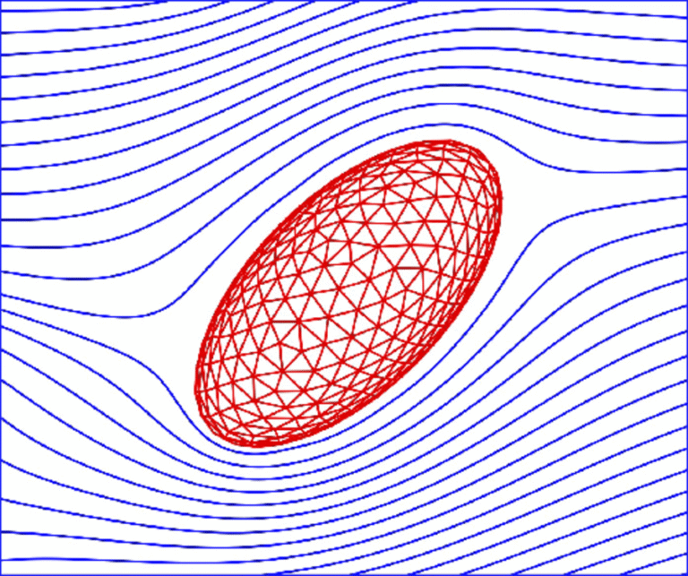
The resulting design can accurately replicate the continuous-phase profile of a spherical lens, even though it’s just a single flat layer. Tests showed that the metalens produced electric field patterns very similar to those of a traditional lens, but in a much thinner and lighter form.
One important design factor was the 1 µm pitch, or spacing, between each meta-atom. The team found that reducing this pitch improved light focusing and reduced diffraction losses. Simulations compared lenses made from silicon (Si) and germanium (Ge), with germanium emerging as the better material due to its higher refractive index, which simplifies fabrication.
Advantages Over Traditional Infrared Systems
This innovation brings several benefits to infrared imaging systems:
- No cryogenic cooling required – The system operates efficiently at room temperature, cutting down cost, power, and complexity.
- Sharper imaging – Focused light on each pixel minimizes optical crosstalk, producing cleaner and more detailed infrared images.
- Compact and lightweight – Being only a single layer thick, these metalenses can be directly integrated onto detector arrays, reducing overall device size and weight.
- Scalable and cost-effective – The metasurface approach is compatible with wafer-scale manufacturing, allowing thousands of lenses to be fabricated simultaneously using standard semiconductor techniques.
These advantages make the technology ideal for continuous, real-time environmental monitoring, as well as defense applications requiring compact, low-power sensors with wide detection range.
Real-World Applications
The TMOS researchers envision several important uses for their technology. One major goal is bushfire detection. Australia’s climate makes it highly prone to devastating wildfires, and current fire monitoring systems can miss small heat sources before they grow out of control. The proposed system could be mounted on telecommunication towers across rural regions, providing 360-degree infrared surveillance that continuously scans for hotspots.
In addition, the same sensors could be used for military and security purposes, giving vehicles, drones, and surveillance equipment better situational awareness with 360-degree coverage. The MWIR band’s ability to detect heat even in total darkness makes it invaluable for night vision, defense monitoring, and threat detection.
Beyond fire and defense, the researchers note that their innovation could impact a wide range of sectors that rely on infrared sensing—such as remote sensing, meteorology, astronomy, spectroscopy, and even medical imaging. In these fields, metalenses could help make infrared equipment smaller, more efficient, and more accessible.
Why the Metalens Approach Matters
Metasurfaces represent one of the most exciting frontiers in optics. Instead of bending light with curved glass, they use nano-scale structures to manipulate light’s phase, amplitude, and polarization. This means a metasurface can do much more than focus light—it can filter, separate, or process it in ways conventional optics can’t.
For instance, a properly designed metalens could split different wavelengths or polarizations, enabling advanced functions like multi-spectral imaging or polarization-sensitive detection within a single, flat component. These capabilities could lead to smarter, more adaptable infrared cameras in the future.
Furthermore, because metasurfaces are made using lithographic methods—the same used for manufacturing computer chips—they’re easy to integrate into existing semiconductor processes, opening the door to mass production and low-cost deployment.
Challenges Ahead
While the results are promising, the current study is primarily based on simulation and modeling, not full physical prototypes. Turning these designs into real-world devices will involve overcoming several engineering hurdles.
Maintaining perfect alignment between the metalens array and detector pixels, ensuring uniform fabrication across large wafers, and minimizing losses due to manufacturing imperfections will all be critical steps. Additionally, while the system operates efficiently without cryogenic cooling, certain detector materials like HgCdTe (Mercury Cadmium Telluride) might still need mild temperature control for best performance.
Nevertheless, the researchers are optimistic. Their findings show that by combining flat optics with infrared sensing, it’s possible to achieve performance on par with traditional systems while dramatically improving practicality and scalability.
Looking Ahead
This breakthrough is more than just an academic exercise—it’s a glimpse of what the future of infrared imaging could look like. Imagine a network of tiny, intelligent sensors spread across forests, mountaintops, or satellites, constantly monitoring for signs of heat anomalies. Such systems could provide early warnings for wildfires, industrial malfunctions, or security threats, all while consuming minimal power and operating under real-world conditions.
As metasurface technology continues to evolve, we can expect to see smaller, faster, and more adaptive optical devices emerging across industries—from defense and space to consumer electronics and environmental safety.
Infrared sensing, once confined to bulky and expensive equipment, may soon become a ubiquitous tool for keeping people and ecosystems safe.
Research Paper: Design and Simulation of Metalens Arrays for Enhanced MWIR Imaging Array Performance – Journal of Electronic Materials (2025)


