Johns Hopkins Scientists Unveil Breakthrough in Microchip Manufacturing with Metal-Organic Chemistry

Researchers at Johns Hopkins University and their global collaborators have reported a major breakthrough in the world of microchip technology.
By harnessing the power of metal-organic materials and a carefully engineered process, the team has demonstrated a way to build microchips so small their features are invisible to the naked eye. This work, recently published in Nature Chemical Engineering, points toward a future of faster, smaller, and more affordable electronics—potentially reshaping industries from smartphones to aerospace.
The Core Discovery
The team focused on one of the biggest challenges in semiconductor manufacturing: creating circuit patterns at ultra-small scales without driving up costs or sacrificing precision. Traditionally, chip makers coat silicon wafers with a radiation-sensitive resist that reacts when exposed to a powerful beam of light or radiation. This process allows intricate circuit patterns to be imprinted on the wafer.
But there’s a problem. As chipmakers push for smaller and smaller features, conventional resists struggle to keep up. The next generation of high-powered radiation, known as beyond extreme ultraviolet radiation (B-EUV), does not interact strongly enough with standard organic resists. That’s where the Johns Hopkins team stepped in with a new solution.
Metal-Organics as a Game-Changer
The researchers discovered that resists made from a new class of metal-organic materials can handle B-EUV exposure. Metals like zinc absorb the radiation effectively, releasing electrons that trigger the necessary chemical reactions in the organic component—an imidazole-based material. This enables the creation of features much smaller than the current 10-nanometer standard.
The exciting part is flexibility. By pairing different metals with different organics, the resist’s efficiency can be tuned. The researchers note that at least 10 metals and hundreds of organics could be explored for this chemistry, offering a wide design space for optimization.
Chemical Liquid Deposition (CLD): A Precise New Method
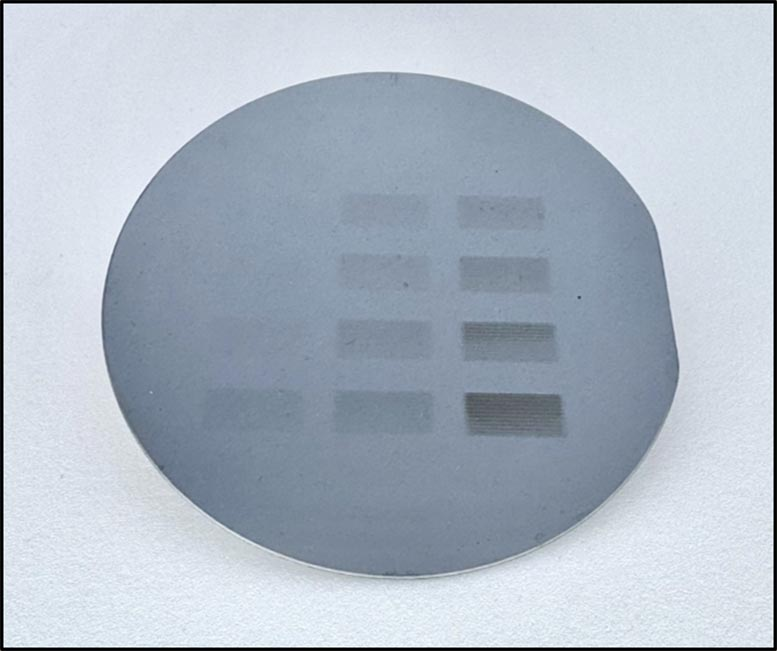
Another major achievement of the project was the development of a new technique called chemical liquid deposition (CLD). Using this method, the team successfully deposited the metal-organic resists on silicon wafers at scale, with nanometer-level control over thickness.
This breakthrough is critical because uniform, wafer-scale deposition is one of the hardest hurdles to overcome in microchip fabrication. The team used both experimental approaches and computational models to refine the process, ensuring accuracy and scalability.
Who’s Involved in the Research
The project is the result of a collaboration spanning multiple institutions:
- Johns Hopkins University (U.S.) – leading the study, with contributions from Yurun Miao, Kayley Waltz, Xinpei Zhou, and Professor Michael Tsapatsis.
- East China University of Science and Technology (China) – researchers Liwei Zhuang, Shunyi Zheng, Yegui Zhou, and Heting Wang.
- Brookhaven National Laboratory (U.S.) – Mueed Ahmad and J. Anibal Boscoboinik.
- Soochow University (China) – Qi Liu.
- École Polytechnique Fédérale de Lausanne (EPFL) (Switzerland) – Kumar Varoon Agrawal.
- Lawrence Berkeley National Laboratory (U.S.) – Oleg Kostko.
This mix of expertise in chemistry, materials science, and engineering was key to solving the multi-layered challenges of developing a new resist system.
Why This Breakthrough Matters
Semiconductors power almost everything around us—phones, computers, cars, appliances, and airplanes. As devices become more powerful, manufacturers face mounting pressure to shrink chip features further while keeping costs manageable.
This discovery matters for several reasons:
- Scaling down features: With the new resist and deposition method, chips can be patterned below 10 nm, pushing past current manufacturing limits.
- Flexibility in design: The approach allows tuning through metal-organic pairings, providing a wide palette of possibilities for optimization.
- Compatibility with B-EUV: This positions the method well for the next 10 years of semiconductor manufacturing, as companies adopt higher-energy radiation for lithography.
- Economic potential: If scalable, the method could lead to cheaper, faster, and more efficient chips, lowering costs across entire industries.
A Closer Look at How Chips Are Made
To understand why this breakthrough is so significant, it helps to review the basics of microchip manufacturing.
- Chips are made from flat slices of silicon wafers.
- These wafers are coated with a resist—a thin, radiation-sensitive layer.
- A high-energy beam (such as ultraviolet light) is directed at the resist, sparking a reaction that etches incredibly fine circuit patterns onto the wafer.
- These circuits are then developed and processed further, eventually becoming the tiny electronic brains inside our devices.
The challenge has always been pushing this process to create smaller features. As the patterns shrink, the wavelengths of light (or radiation) used to etch them must also shrink. That’s why the industry has moved from deep ultraviolet (DUV) to extreme ultraviolet (EUV), and now researchers are exploring B-EUV for even higher resolution.
Limitations of Current Approaches
While EUV lithography has been a monumental achievement, it faces bottlenecks:
- Conventional resists don’t absorb EUV or B-EUV strongly enough, limiting resolution.
- Cost and throughput become major concerns when trying to scale new technologies.
- Optics and radiation sources for shorter wavelengths require advanced infrastructure, making them extremely expensive.
By introducing a resist that works better with B-EUV, the Johns Hopkins team provides a potential way forward—though challenges remain before this method can be fully industrialized.
Looking Toward the Future
The researchers have already begun experimenting with different metal-organic combinations to fine-tune the chemistry for B-EUV. They predict that as semiconductor manufacturing shifts toward B-EUV in the next decade, this chemistry will be well-positioned for adoption.
The team also highlighted an important detail: a metal that performs poorly under one wavelength might excel under another. For example, zinc isn’t particularly effective under EUV, but under B-EUV, it becomes one of the best candidates. This adaptability underscores the strength of the approach.
Extra Insight: What Exactly is B-EUV?
The term B-EUV (beyond extreme ultraviolet) refers to radiation with a wavelength shorter than EUV’s standard 13.5 nanometers. Going beyond this limit allows even finer chip features, potentially down to single-digit nanometer scales.
However, shorter wavelengths bring huge challenges:
- Generating the radiation requires specialized, highly energetic light sources.
- Handling the optics (mirrors and lenses) becomes far more complex.
- Resists must be carefully engineered to respond effectively at these wavelengths.
This is why new resist chemistries, like the metal-organic systems explored here, are such a critical piece of the puzzle.
Broader Context: The Semiconductor Industry’s Race
The push for smaller chips is part of a long trend known as Moore’s Law, which observed that the number of transistors on a chip tends to double roughly every two years. While Moore’s Law has slowed in recent years, the drive for denser, more powerful chips continues.
Tech giants like Intel, TSMC, and Samsung are all investing heavily in EUV and next-generation lithography. Breakthroughs like this one could play a role in shaping their roadmaps, though large-scale adoption depends on practical challenges like cost, throughput, and reliability.
Key Challenges Ahead
Despite the excitement, several hurdles remain before this approach can revolutionize chipmaking:
- Industrial scaling: Lab-scale success must be replicated at massive production levels.
- Durability: Metal-organic resists must withstand processing conditions and environmental factors.
- Integration: New materials must work seamlessly with existing semiconductor processes.
- Competition: Other advanced lithography methods (like multi-beam electron lithography or directed self-assembly) are also being pursued.
Nevertheless, this work lays a strong foundation for future exploration.
Conclusion
The discovery from Johns Hopkins and its collaborators highlights a powerful new path for microchip manufacturing. By combining metal-organic chemistry with a scalable deposition method, the researchers have opened the door to sub-10 nm features, compatibility with B-EUV lithography, and potentially faster, cheaper, more efficient chips.
As industries continue to demand more computing power in smaller, more affordable packages, breakthroughs like this one could define the next decade of technology. While challenges remain, the groundwork laid here is a promising step toward the future of semiconductors.
Research Reference: Spin-on deposition of amorphous zeolitic imidazolate framework films for lithography applications – Nature Chemical Engineering (2025)


