New Light-Based Chip Promises Up to 100x More Efficient AI

Artificial intelligence has grown at an astonishing pace in recent years, but there’s a growing problem: energy consumption. The computational load from training and running AI models is pushing electricity demand higher than ever. Now, researchers from the University of Florida, along with collaborators at the Florida Semiconductor Institute, UCLA, and George Washington University, have introduced something that could change the game — a new chip that uses light instead of electricity to perform some of AI’s most energy-hungry tasks.
This breakthrough was published in Advanced Photonics on September 8, 2025, and it revolves around a technique that integrates lasers and miniature lenses directly onto a chip. The goal? To slash power usage while maintaining the same level of accuracy as conventional processors.
What Makes This Chip Different?
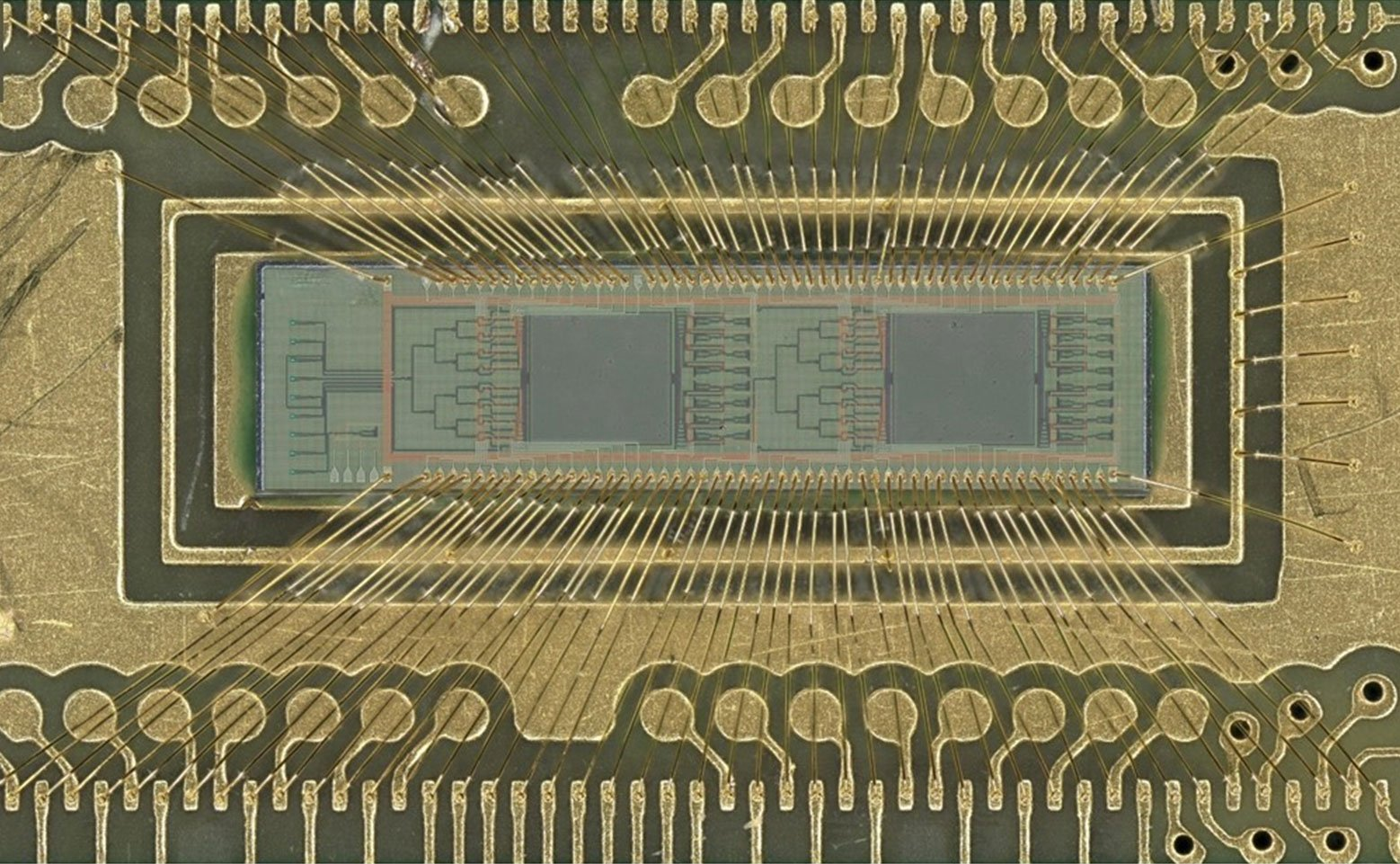
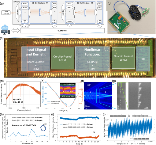
At the heart of this design is the shift from electrical signals to optical signals. Instead of moving electrons through circuits, the chip converts data into laser light, pushes it through tiny lenses, and then converts it back to a digital signal.
These lenses are based on Fresnel designs — the same concept used in lighthouses, but here they are shrunken down to a fraction of the width of a human hair. These minuscule lenses are manufactured using standard semiconductor processes, meaning the chip can potentially be mass-produced without exotic equipment.
By using light, the chip avoids the resistive losses that come with electrical current. This makes calculations more efficient, faster, and significantly less energy-hungry.

Why Focus on Convolution?
One of the chip’s primary strengths lies in performing convolutions, which are mathematical operations central to how AI processes information.
- Image recognition: Convolution layers scan over images to identify features such as edges, textures, and shapes.
- Video analysis: Frames are analyzed in a similar way, detecting motion and patterns.
- Language models: Even written text relies on convolution for detecting patterns in sequences of words and characters.
Currently, convolution is one of the most computationally expensive parts of AI workloads. This is why reducing its cost is a huge win. The new light-based chip handles convolution using a method called a photonic joint transform correlator (pJTC). This allows it to perform Fourier transforms — a crucial part of convolution — naturally, just by letting light pass through lenses.
The result is a dramatic improvement in both efficiency and speed.
Performance and Accuracy
In early trials, the chip was tested on recognizing handwritten digits (using the MNIST dataset, a common benchmark in AI research). The chip reached about 98% accuracy, which matches the performance of traditional electronic chips.
But the real story is in efficiency:
- The design is estimated to achieve up to 305 TOPS/W (trillions of operations per second per watt).
- It also offers 40.2 TOPS per mm² in terms of area efficiency.
- In practice, this means the chip could be 10x to 100x more efficient than existing hardware when handling convolution operations.
This is not just a marginal upgrade. It represents an entirely new way of approaching AI hardware.

Parallel Processing with Light
Another advantage of using light is the ability to exploit different wavelengths. Multiple colors of laser light can pass through the same lens at the same time, each carrying different data streams.
This is called wavelength-division multiplexing, and it allows the chip to process parallel data streams far more efficiently than conventional processors. Instead of just scaling chips by making transistors smaller (which is hitting physical limits), this design adds a new dimension of scalability.
How It’s Built
The chip uses two sets of miniature Fresnel lenses integrated directly onto the semiconductor substrate. These lenses act as optical processors that carry out Fourier transforms — a key mathematical step in convolution.
Here’s the workflow:
- Data input (such as an image or pattern recognition task) is converted into laser light.
- The light passes through the Fresnel lenses, where convolution is performed optically.
- The output light is then converted back into a digital electrical signal for further AI processing.
Because the convolution happens while light propagates, energy use is almost negligible. This is why researchers describe the operation as near-energy-free photonic Fourier transformation.
Who Is Behind This Work?
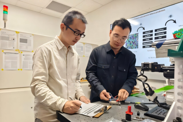
The study was led by Volker J. Sorger, the Rhines Endowed Professor in Semiconductor Photonics at the University of Florida. His team has been working on ways to merge photonics and electronics to improve AI efficiency.
Hangbo Yang, a research associate professor at UF and co-author, highlighted the novelty of applying optical computation directly to AI neural networks on-chip — something that hasn’t been done before at this scale.
The collaboration involved experts from multiple institutions, showing the interdisciplinary push behind optical computing.
Why This Matters for AI’s Future
AI has a power problem. Training large models already consumes megawatt-hours of electricity, and inference (running the models for tasks like chatbots, image recognition, and translation) continues to add to the load.
If AI adoption keeps growing, it could put serious strain on power grids worldwide. That’s why hardware breakthroughs like this are so important.
Optical chips like this one could:
- Enable more advanced AI models without skyrocketing energy costs.
- Make AI more sustainable in the long run.
- Open the door to smaller, low-power edge devices that can still run sophisticated AI locally.
Potential Industry Impact
It’s worth noting that major chip companies such as NVIDIA already use some optical elements in their AI systems, mostly for interconnects. The addition of optical convolution could be a natural next step.
If this design proves scalable, it might not be long before every AI chip includes optical components alongside traditional transistors. The researchers behind this project suggest that optical AI computing will become a mainstream feature in future hardware.
Challenges Ahead
Of course, this is still an early-stage prototype. There are several challenges before it can reach commercial deployment:
- Scaling: The current tests have been limited to smaller AI tasks, like handwritten digit recognition. Scaling to more complex models will require further development.
- Integration: Optical convolution is just one piece of an AI pipeline. Other elements — such as nonlinear activation functions, pooling, and memory management — must still be handled electronically.
- Manufacturability: While the chip uses mostly standard semiconductor processes, introducing new photonic design kits and ensuring high yields at scale will take time.
Despite these hurdles, the proof of concept is strong enough to signal that optical AI accelerators may soon move from labs to industry.
A Quick Detour: What Is Optical Computing?
Since we’re on the topic, let’s take a moment to understand the broader field of optical computing.
Optical computing refers to using photons (particles of light) instead of electrons to perform calculations. The benefits are clear:
- Speed: Light travels faster than electrical signals and can carry more information.
- Parallelism: Multiple wavelengths (colors) of light can be used simultaneously to process different tasks in parallel.
- Energy efficiency: Light doesn’t suffer from the same resistive heating losses that plague electronics.
However, building fully optical computers has been a challenge for decades. The difficulty lies in creating reliable, programmable devices that can handle a wide range of tasks, not just specialized ones.
This new AI chip shows that hybrid designs — combining the best of optics with electronics — may be the most practical path forward.
Fresnel Lenses: The Secret Weapon
A particularly clever detail in this design is the use of Fresnel lenses. Traditionally, these lenses were used in lighthouses because they could bend and focus light efficiently without requiring large amounts of glass.
In this chip, the same principle is applied at a microscopic scale. The result is lenses that are just a fraction of a hair’s width but powerful enough to manipulate laser light for AI computations.
This approach is elegant because it uses well-understood optical principles in a completely new context.
The Bigger Picture
If successful, this technology could redefine the balance between electronics and photonics in computing. For decades, Moore’s Law (the idea that the number of transistors on a chip doubles every two years) has driven progress. But transistor miniaturization is now approaching physical limits.
Optical computing doesn’t rely on shrinking transistors — instead, it opens up a new way of thinking about computation. By offloading certain operations, like convolution, to light-based systems, chips can achieve far greater efficiency.
The potential applications go beyond AI:
- Medical imaging: Faster and more energy-efficient processing of scans.
- Signal processing: Telecommunications could benefit from rapid, low-power data analysis.
- Scientific computing: Simulations and pattern recognition tasks could see significant boosts.
Final Thoughts
This light-based AI chip is still in the experimental stage, but it represents a leap forward in how we think about AI hardware. By combining lasers, Fresnel lenses, and silicon photonics, researchers have shown that it’s possible to achieve near-zero energy convolution — one of the heaviest parts of AI computation.
With an efficiency boost of 10x to 100x, and the ability to run multiple wavelengths in parallel, this design could soon reshape the landscape of AI hardware. While challenges remain, the potential is too significant to ignore.
As AI continues to expand into every part of our lives, breakthroughs like this will be critical in making sure progress is both powerful and sustainable.
Research Reference: Near-energy-free photonic Fourier transformation for convolution operation acceleration, published in Advanced Photonics, September 8, 2025.


