The End of Silicon? Penn State Scientists Build the World’s First 2D Material-Based Computer

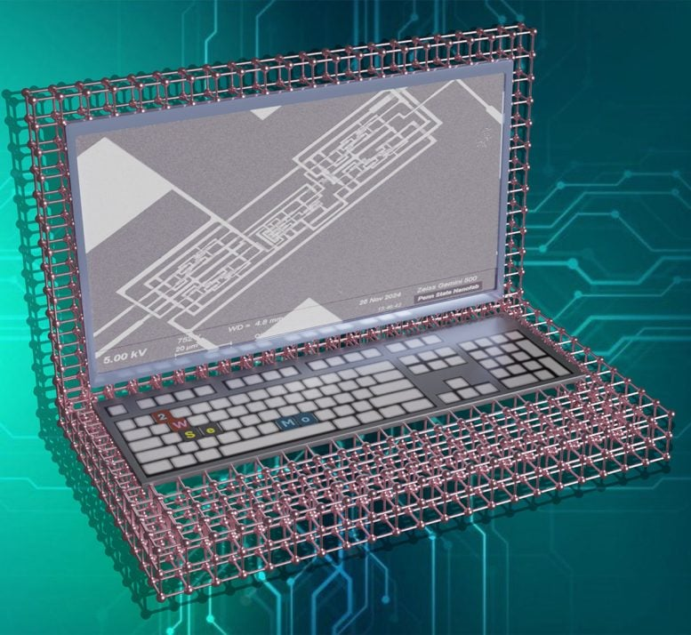
A research team at Pennsylvania State University has achieved something that could mark the beginning of a new chapter in computing — the creation of the world’s first computer built entirely from two-dimensional (2D) materials, completely free of silicon. This new system, described as a 2D complementary metal–oxide–semiconductor (CMOS) computer, represents a significant leap toward more efficient, thinner, and potentially revolutionary forms of electronics.
Below is a clear and detailed breakdown of what this breakthrough involves, how it was achieved, and why it matters for the future of technology.
What Exactly Did the Penn State Team Build?
The Penn State researchers designed and fabricated a functioning computer that operates using 2D materials instead of traditional silicon. These materials are just one atom thick, yet they maintain exceptional electrical properties even at that incredibly thin scale.
In conventional computing, silicon has been the bedrock material for decades. Every smartphone, laptop, and server relies on billions of silicon-based transistors to perform logic operations. However, as engineers try to make transistors smaller and faster, silicon is beginning to hit physical limits — it loses efficiency and generates more heat as it shrinks.
The Penn State team, led by Professor Saptarshi Das and doctoral researcher Subir Ghosh, has shown that two-dimensional materials can take us beyond these limits. Their project demonstrates a fully working CMOS computer, made entirely from atom-thin transistors using molybdenum disulfide (MoS₂) and tungsten diselenide (WSe₂) — two materials with distinct electrical properties ideal for building transistors.
The Core of the Breakthrough: 2D CMOS Technology
To understand the importance of this work, it helps to look at how CMOS technology works. A CMOS circuit relies on two types of transistors — n-type and p-type — that work together to manage the flow of electric current efficiently. This combination allows for low power consumption, high performance, and stability, which is why CMOS is used in virtually every modern electronic device.
In this case, the Penn State team replaced the silicon-based transistors with 2D materials:
- Molybdenum disulfide (MoS₂) for n-type transistors.
- Tungsten diselenide (WSe₂) for p-type transistors.
By combining these materials, the team created a complete CMOS system — not just isolated transistors or small circuits, but a fully functional computer capable of executing logic operations.
How They Made It: The Fabrication Process
The researchers used a process called metal–organic chemical vapor deposition (MOCVD) to grow large, uniform sheets of the 2D materials. This method involves vaporizing compounds, allowing them to chemically react and deposit as thin layers on a surface — in this case, forming atom-thick films of MoS₂ and WSe₂.
They then fabricated over 1,000 transistors of each type (n-type and p-type) and precisely adjusted their threshold voltages — the voltage levels required to switch them on and off. This tuning allowed the team to integrate the transistors into fully operational CMOS logic circuits.
To make everything work in harmony, they optimized several steps of the device fabrication process, including post-processing treatments to balance electron and hole transport across the two materials.
The result was a functioning silicon-free computer, capable of executing operations based on a one instruction set computer (OISC) architecture — a simplified computing model that can perform universal computation using only one instruction.
How Powerful Is It?
Let’s set expectations clearly. This prototype doesn’t compete with your laptop’s processor — not yet.
The 2D CMOS computer currently runs at a maximum frequency of 25 kilohertz (kHz), compared to billions of operations per second (gigahertz range) in typical silicon processors. However, that’s not the point of this breakthrough. The key achievement is that the researchers demonstrated complete functionality using 2D materials, something no one had managed before.
The computer operates on very low supply voltages and minimal power consumption, with switching energies measured in picojoules — orders of magnitude lower than what conventional chips use.
This early system is a proof of concept, demonstrating that complex logic circuits and full CMOS operation are possible using materials only a few atoms thick. The next challenge is to make these systems faster, more scalable, and practical for real-world applications.
Modeling and Performance Evaluation
To predict how their 2D computer might perform when scaled up, the team created a computational model based on SPICE simulations. They calibrated the model with real experimental data and included device-to-device variations to make the simulations accurate.
Using this model, they compared their 2D CMOS design with state-of-the-art silicon technology, projecting how improvements in fabrication and design could close the performance gap in future generations. The findings suggest that, while the 2D devices currently operate slower, they have the potential to surpass silicon in energy efficiency and miniaturization.
Why This Matters
The implications of this work go far beyond one experimental chip. Here’s why it matters:
- End of Silicon Scaling – For decades, Moore’s Law (the idea that transistor counts double roughly every two years) has been fueled by silicon miniaturization. But as transistor dimensions reach atomic scales, silicon begins to suffer from quantum leakage and heat dissipation problems. 2D materials, however, can remain stable and efficient at atomic thickness.
- Energy Efficiency – As our world demands more computing power — from AI systems to data centers — energy consumption has become a major concern. 2D materials could drastically reduce power requirements because they can operate at much lower voltages.
- Flexibility and New Applications – Atom-thin materials can be bent, stretched, or integrated onto unconventional surfaces, opening the door to flexible, wearable, or even transparent electronics. Imagine computers built into fabrics or ultra-thin sensors that adhere to skin or glass.
- Long-Term Potential – This isn’t an overnight revolution, but it’s the kind of foundational advance that often sparks one. Silicon took nearly 80 years to evolve from lab experiments to the backbone of global computing. Research into 2D materials only began around 2010, so achieving a working 2D CMOS computer in just over a decade is an impressive trajectory.
The Team Behind the Breakthrough
The project was led by Professor Saptarshi Das, an expert in 2D electronics and the Ackley Professor of Engineering Science and Mechanics at Penn State, along with Subir Ghosh, the first author and a doctoral student in the same department.
Their collaborators included graduate students Yikai Zheng, Najam U. Sakib, Harikrishnan Ravichandran, Yongwen Sun, Andrew Pannone, Muhtasim Ul Karim Sadaf, and Samriddha Ray, as well as Yang Yang, an assistant professor affiliated with both the Materials Research Institute and the Department of Nuclear Engineering at Penn State.
The team also worked closely with Joan Redwing, director of the 2D Crystal Consortium Materials Innovation Platform (2DCC-MIP) at Penn State, and Chen Chen, an assistant research professor. Additional collaborators included researchers Musaib Rafiq and Subham Sahay from the Indian Institute of Technology, and Mrinmoy Goswami from Jadavpur University.
Funding came from the U.S. National Science Foundation (NSF), the Army Research Office, and the Office of Naval Research.
A Closer Look at 2D Materials
Since the breakthrough involves 2D materials, let’s take a quick look at what they are and why they’re so special.
Two-dimensional materials are crystalline substances consisting of a single layer of atoms. The most famous example is graphene, a single layer of carbon atoms arranged in a hexagonal lattice. After graphene’s discovery in 2004, scientists began exploring hundreds of similar materials, such as molybdenum disulfide (MoS₂), tungsten diselenide (WSe₂), and hexagonal boron nitride (h-BN).
These materials have exceptional mechanical strength, thermal conductivity, and electronic mobility, even at atomic thickness. In contrast to silicon, which becomes unstable when thinned down too far, 2D materials retain their properties — making them ideal candidates for ultra-miniaturized electronics.
Molybdenum disulfide (MoS₂) is known for its ability to act as a semiconductor with a suitable bandgap for transistors, while tungsten diselenide (WSe₂) serves as a complementary p-type semiconductor, making the pair perfect for CMOS logic design.
What Comes Next?
Although the Penn State computer is slow by today’s standards, it opens an exciting frontier. The team plans to optimize the fabrication process, reduce parasitic capacitance, and improve contact interfaces to increase operating speed.
Scaling up 2D computers will also involve developing new manufacturing techniques to grow larger, defect-free 2D films and to integrate them into multi-layer systems. Eventually, such technologies could merge with existing silicon processes, forming hybrid chips that combine the strengths of both worlds.
We might see the first practical applications in low-power sensing, flexible displays, or wearable medical devices, where ultra-thin form factors and minimal energy use are more valuable than raw processing power.
Why This Discovery Deserves Attention
This isn’t a flashy gadget for sale next year — it’s a deep scientific milestone. Building a fully functional silicon-free computer demonstrates that 2D materials are no longer a futuristic dream; they are entering the realm of practical electronic systems.
It’s also a reminder that technological revolutions start with small, proof-of-concept experiments. The first silicon transistors in the 1950s were slower and less reliable than vacuum tubes. Within decades, they redefined everything from space exploration to smartphones.
The same could happen here. While the silicon era isn’t ending overnight, this research shows that its successor may already be taking shape in the lab.
Reference: A complementary two-dimensional material-based one instruction set computer – Nature, 11 June 2025


